

Semiconductor device and method of manufacturing the same
- Summary
- Abstract
- Description
- Claims
- Application Information
AI Technical Summary
Benefits of technology
Problems solved by technology
Method used
Image

Examples
experiment 1
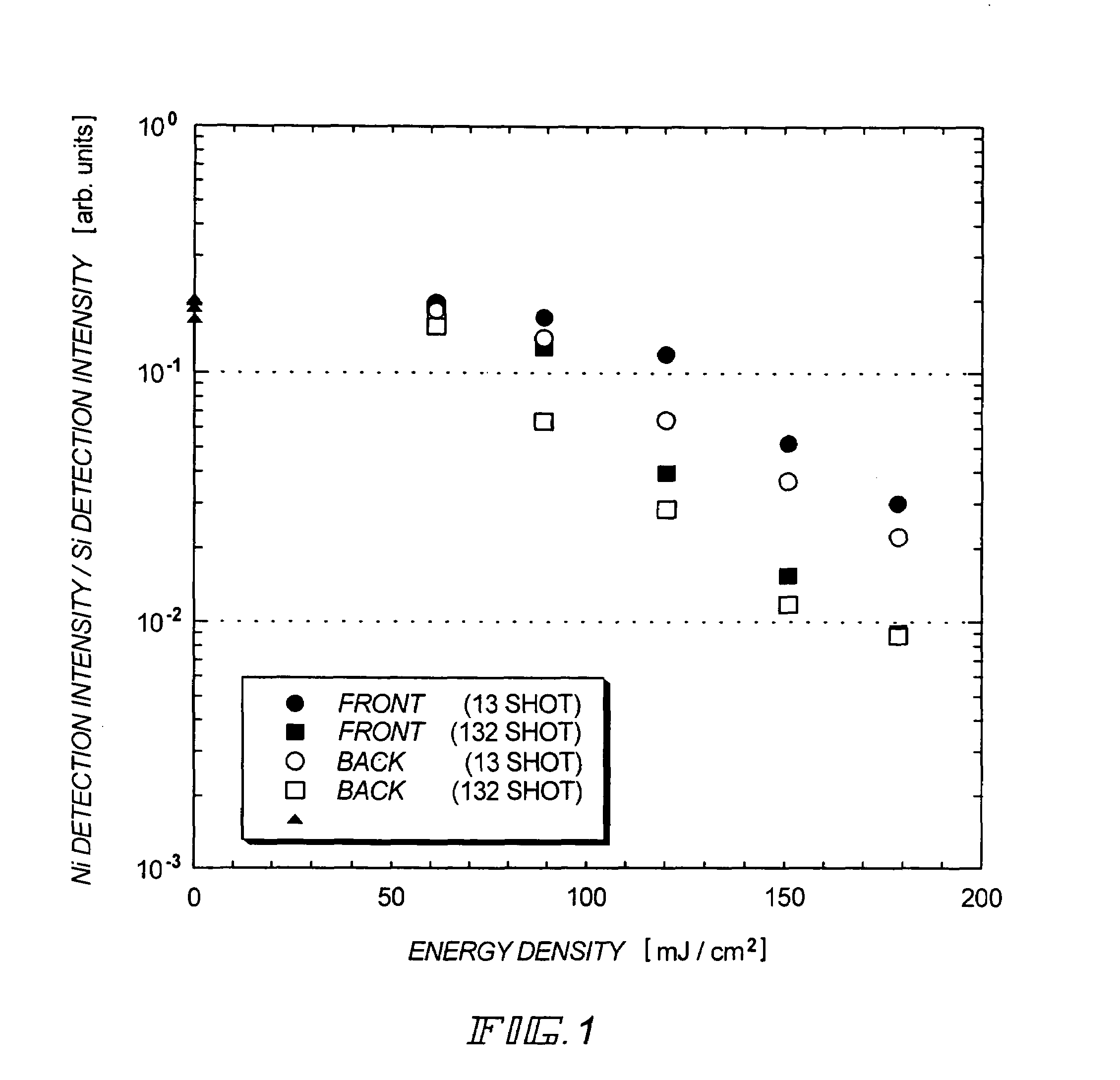
[0078]First, a silicon oxide film with a thickness of 280 nm and an amorphous silicon film with a thickness of 69 nm are formed by reduced pressure thermal CVD and layered on a quartz substrate and a nickel acetate aqueous solution (5 ppm) is applied thereto to prepare a sample. While laser light conditions are varied (including the energy density and the number of shots), samples are irradiated with laser light. Then, the nickel detection intensity and the silicon detection intensity on the surfaces are measured by TXRF (total reflection X-ray fluorescence) to calculate the ratio of the nickel detection intensity to the silicon detection intensity. Experiment 1 is an experiment for examining the presence or absence of a change in nickel concentration immediately after irradiating the laser light.
[0079]FIG. 1 shows the results of Experiment 1. In FIG. 1, samples irradiated with excimer laser light (energy density: 60 mJ / cm2, 90 mJ / cm2, 120 mJ / cm2, 150 mJ / cm2, 180 mJ / cm2) of 132 shot...
experiment 2
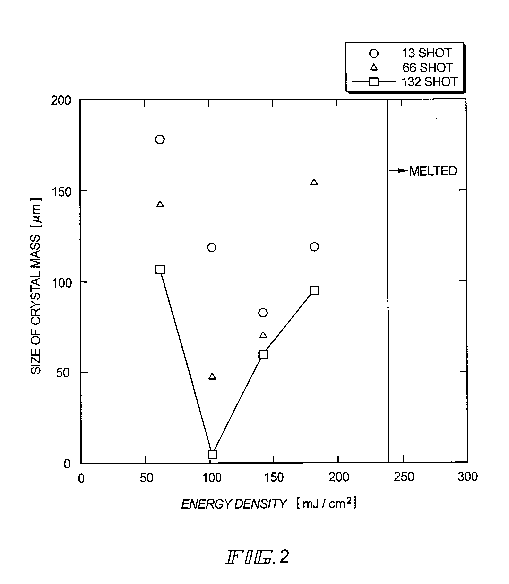
[0080]The samples irradiated with laser light from the back side in Experiment 1 are subjected to heat treatment (heat treatment at 450° C. for an hour which is followed by heat treatment at 600° C. for twelve hours) for crystallization. The samples are then observed through an optical microscope to measure sizes of crystal masses. Experiment 2 is an experiment for examining the relation between the size of the crystal mass and the energy density in the case where irradiation of laser light from the back side precedes heat treatment for crystallization.
[0081]FIG. 2 shows the results of Experiment 2. In FIG. 2, samples irradiated with excimer laser light (energy density: 60 mJ / cm2, 90 mJ / cm2, 120 mJ / cm2, 120 mJ / cm2, 180 mJ / cM2) of 132 shots from the back side of the substrate are plotted and indicated by □. Samples irradiated with excimer laser light (energy density: 60 mJ / cm2, 90 mJ / cm2, 120 mJ / cm2, 150 mJ / cm2, 180 mJ / cm2) of 13 shots from the back side of the substrate are plotted ...
embodiment 1
[Embodiment 1]
[0097]Embodiment 1 describes an example of manufacturing a TFT from an amorphous semiconductor film obtained by reduced pressure thermal CVD on a quartz substrate (1.1 mm in thickness). The description is given with reference to FIGS. 4A to 4G.
[0098]First, an amorphous silicon film 101 with a thickness of 50 nm and a silicon oxide film 102 with a thickness of 50 nm are formed on each side of a quartz substrate 100 by reduced pressure thermal CVD (FIG. 4A).
[0099]A resist film 103 is formed next in order to remove the amorphous silicon film and silicon oxide film formed on the back side of the substrate. The silicon oxide film on the back side is removed by a solution containing fluoric acid, and the amorphous silicon film on the back side is removed by a mixture gas of SF6 and He (FIG. 4A).
[0100]Next, the resist film 103 is removed and the silicon oxide film 102 on the front side is removed. After washing the substrate with diluted fluoric acid, an oxide film (not shown...
PUM
 Abstract
Description
Claims
Application Information