Semiconductor device with a short-lifetime region and manufacturing method thereof

a technology of short-life region and manufacturing method, which is applied in the manufacture of final products, basic electric elements, climate sustainability, etc., can solve the problems of insufficient di/dt capability of high surge, damage to the diode, and inability to obtain di/dt capability, etc., to achieve high di/dt capability and increase forward voltage

Active Publication Date: 2005-12-01
FUJI ELECTRIC CO LTD
View PDF2 Cites 17 Cited by
  • Summary
  • Abstract
  • Description
  • Claims
  • Application Information

AI Technical Summary

Benefits of technology

[0026] As the short-lifetime region is provided over the surface of the chip in the region from a position shallower than the p-n junction surface with a depth of 12.6 μm or greater to a position deeper than the p-n junction surface, a sufficiently high di / dt capability can be obtained against a surge such as a lightening surge without considerably increasing the forward voltage VF.

Problems solved by technology

In the reverse recovery operation mode of the diode, heat generation due to current excessively concentrated in a peripheral section of a chip results in damage of the diode.
Therefore, the di / dt capabilities obtained by the technologies described in the above references are insufficient for the di / dt of a high surge such as a lightening surge.
However, no di / dt capability can be obtained that is sufficiently high to such an extent that the chip can withstand a lightening surge.
This therefore complicates the manufacturing process, resulting in an increase in a chip cost.
In addition, even though a region with a short lifetime of carriers is locally formed in the depth direction on the surface of the chip or in its vicinity by using He ions or protons, no sufficient di / dt capability can be obtained.
Further, in the case of diffusing heavy metal as a lifetime killer, there is difficulty in controlling the diffusion depth of the heavy metal.

Method used


Image

  • Semiconductor device with a short-lifetime region and manufacturing method thereof
  • Semiconductor device with a short-lifetime region and manufacturing method thereof
  • Semiconductor device with a short-lifetime region and manufacturing method thereof

Examples


Embodiment Construction

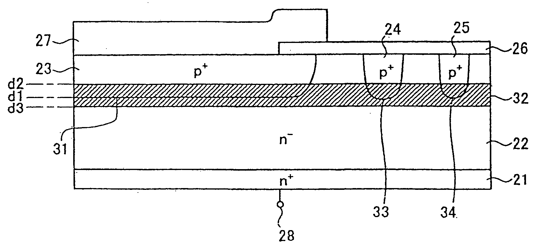
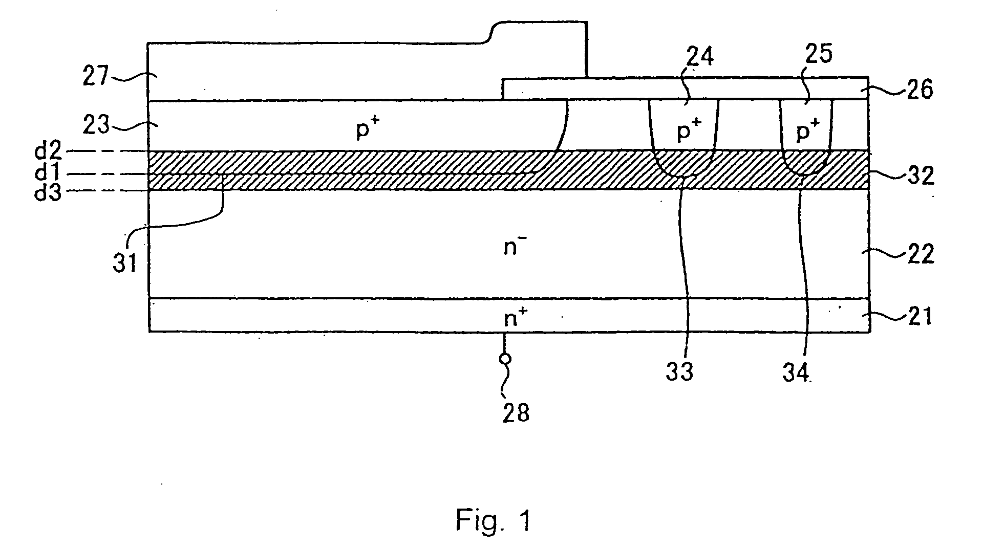
[0035] After extensive studies, the present inventors have discovered that, by presenting an area with a shortened lifetime of carriers over the whole surface of a chip in an area ranging from a position shallower than a p-n junction to a position deeper than the junction, a sufficiently high di / dt capability can be obtained against a surge, such as a lightening surge. Moreover, the present inventors also discovered that, with the p-n junction surface provided deep to some extent, a sufficiently high di / dt capability can be obtained against a surge such as a lightening surge. The invention has been made on the basis of such findings.

[0036] In the following, preferred embodiments of a semiconductor device and a method of manufacturing the device according to the invention will be explained in detail with reference to the attached drawings.

[0037]FIG. 1 is a cross sectional view showing a structure of a planar PIN diode according to the embodiment of the invention. As shown in FIG. 1...


PUM


Abstract

A semiconductor device has an n-semiconductor layer and p+-diffusion regions each having a depth of 14 to 20 μm (design value) selectively formed in the n semiconductor layer. With the entire surface of the chip irradiated with light ions, such as He ions, a lifetime killer is introduced from a position d2 shallower than a position d1 of a p-n junction surface, formed from the n-semiconductor layer and the p+-diffusion regions, to a position d3 deeper than the position d1 to form a short-lifetime region over the entire chip. The irradiation is carried out so that the light ion irradiation half width is not more than the depth of the p+-diffusion regions and a position of a peak of the light ions becomes deeper than the light ion irradiation half width and within the range between 80% and 120% of the depth of the p+-diffusion regions. Thus, in a semiconductor device such as a converter diode, a capability for a high decay rate of a reverse recovery current di/dt can be brought sufficiently high to such an extent that the device can withstand a lightening surge with a low forward voltage VF being kept low.

Description

BACKGROUND [0001]FIG. 6 is a circuit diagram showing an example of an automobile power module. As shown in FIG. 6, the power module is provided with a converter section 1, a break section 2, an inverter section 3, and a thermistor 4. The converter section 1 has converter diodes 5 each ordinarily made of a PIN diode. For example, for a module with a rated voltage of 1200V or 600V, a PIN diode with a breakdown voltage of 1600V or above or 800V or above is used, respectively, as a converter diode 5. The reason that the breakdown voltage is above the rated voltage is because the voltage higher than the rated voltage is sometimes applied to the module. This protects the PIN diode against breakdown in such a case. Moreover, in the PIN diode used as the converter diode 5, the diode 5 needs to have a low forward voltage VF. For example, in a converter diode 5 with a module rated voltage of 1200V, a required value for the forward voltage VF is on the order of 1.2 to 1.5 V. [0002]FIG. 7 is a ...

Claims


Application Information

Patent Timeline
Patent Type & Authority Applications(United States)
IPC IPC(8): H01L29/861H01L21/00H01L21/265H01L29/32H01L29/78H01L31/00H01L31/0264H01L31/105H01L31/18
CPCH01L31/0264Y02E10/50H01L31/186H01L31/105H01L29/0619H01L29/32H01L29/868Y02P70/50
Inventor MATSUI, TOSHIYUKIHOSHI, YASUYUKIKOBAYASHI, YASUYUKIMIYASAKA, YASUSHI
Owner FUJI ELECTRIC CO LTD
Why Eureka
Try Eureka