
Semiconductor storage device

a storage device and semiconductor technology, applied in the direction of information storage, static storage, digital storage, etc., can solve the problems of inability to rewrite data acquired after assembly, inability to replace memory cells in faulty areas, and inability to be rewritten by users, etc., to achieve the effect of lowering the development cos

Inactive Publication Date: 2005-12-01
PANASONIC CORP
View PDF7 Cites 1 Cited by
  • Summary
  • Abstract
  • Description
  • Claims
  • Application Information

AI Technical Summary

Benefits of technology

[0011] The present invention has been conceived in light of the foregoing problem and aims at providing a semiconductor storage device which can adapt to assembly processes involving different treatment temperatures, can become unrewritable when rewriting of data by the user is prohibited, negates the necessity for developing different semiconductor storage devices, and lowers development cost.
[0033] If the heat treatment in the assembly processes falls within the temperature range at which data in the nonvolatile memory are guaranteed, the ability to replace a memory cell in a faulty area after assembly is desirable for further enhancing a yield. For this reason, the faulty address information and the mode setting data are stored in the nonvolatile memory, and setting can be made such that the faulty address information and the operation mode setting information are transferred from the electrically-rewritable nonvolatile memory.
[0035] Specifically, according to the present invention, the semiconductor storage devices of (1) to (4) can be embodied by means of a single semiconductor storage device, whereby a period and cost of development can be curtailed.
[0036] (1) A high-security semiconductor storage device-which enables replacement of a memory cell in a faulty area with high reliability and which prevents the user from rewriting operation mode data and faulty address data—can be embodied by means of storing the faulty address data and the operation mode data in once-rewritable nonvolatile memory.
[0037] (2) A semiconductor storage device—which has a high degree of freedom in replacement of a memory cell in a faulty area after assembly and enables flexible setting of an operation mode—can be embodied by means of storing the faulty address data in the once-rewritable nonvolatile memory and storing operation mode data in electrically-rewritable nonvolatile memory.

Problems solved by technology

In relation to a related-art semiconductor storage device, when the temperature of heat treatment performed during an assembly processes falls outside a guaranteed temperature at which a memory cell can latch data, replacement of a memory cell in a faulty area becomes impossible.
Moreover, there may be a case where storing operation modes or a faulty address in memory (mask ROM or the like) which cannot be rewritten by the user is desired.
Such mask ROM or the like is not affected by the temperature of heat treatment during the assembly process, but the data acquired after assembly are unrewritable.
The related-art semiconductor storage device cannot satisfy the foregoing competing requirements simultaneously.
Different semiconductor devices must be developed in response to the respective desires, raising a problem of an increase in development cost.

Method used


Image

  • Semiconductor storage device
  • Semiconductor storage device
  • Semiconductor storage device

Examples


first embodiment

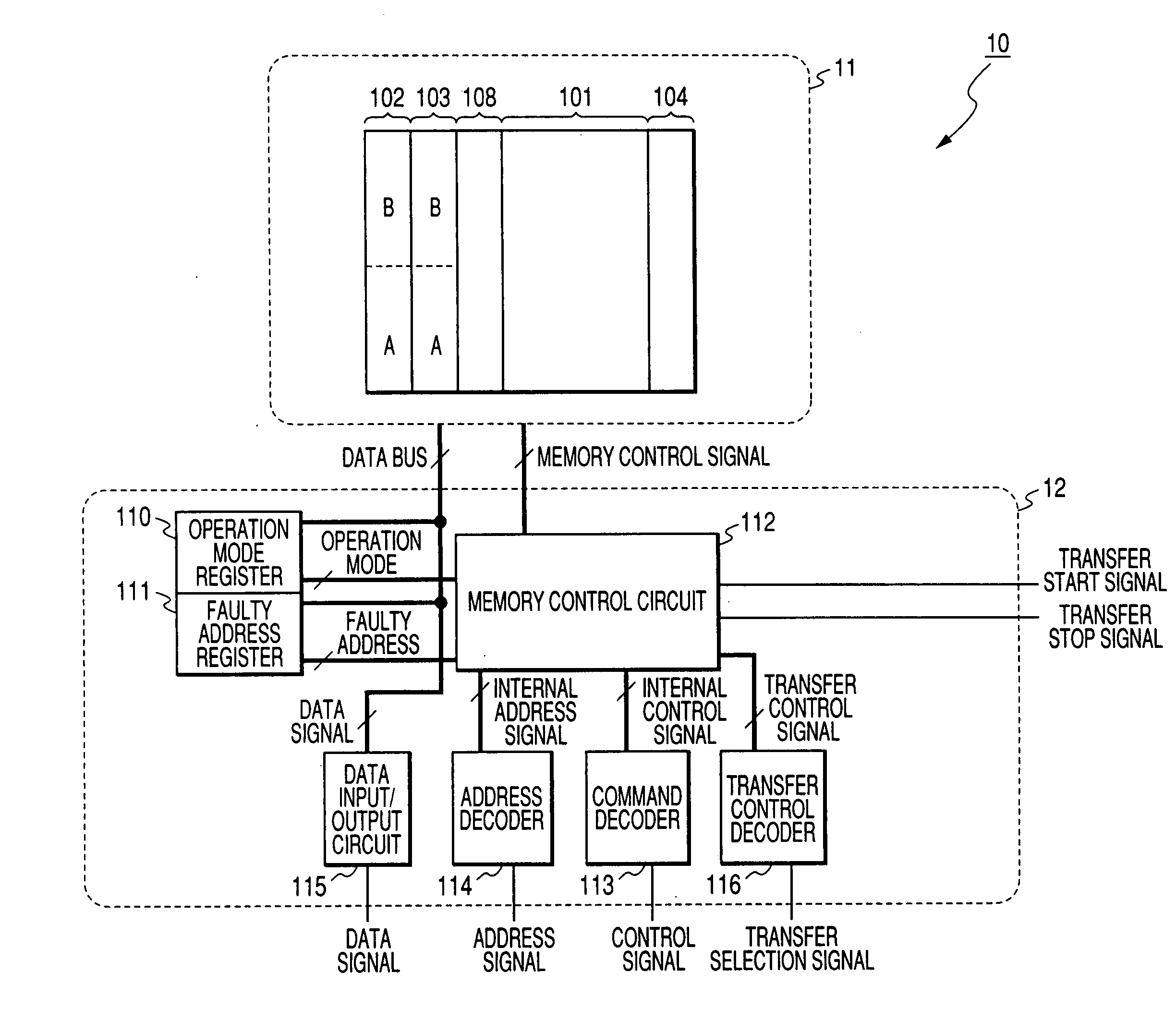
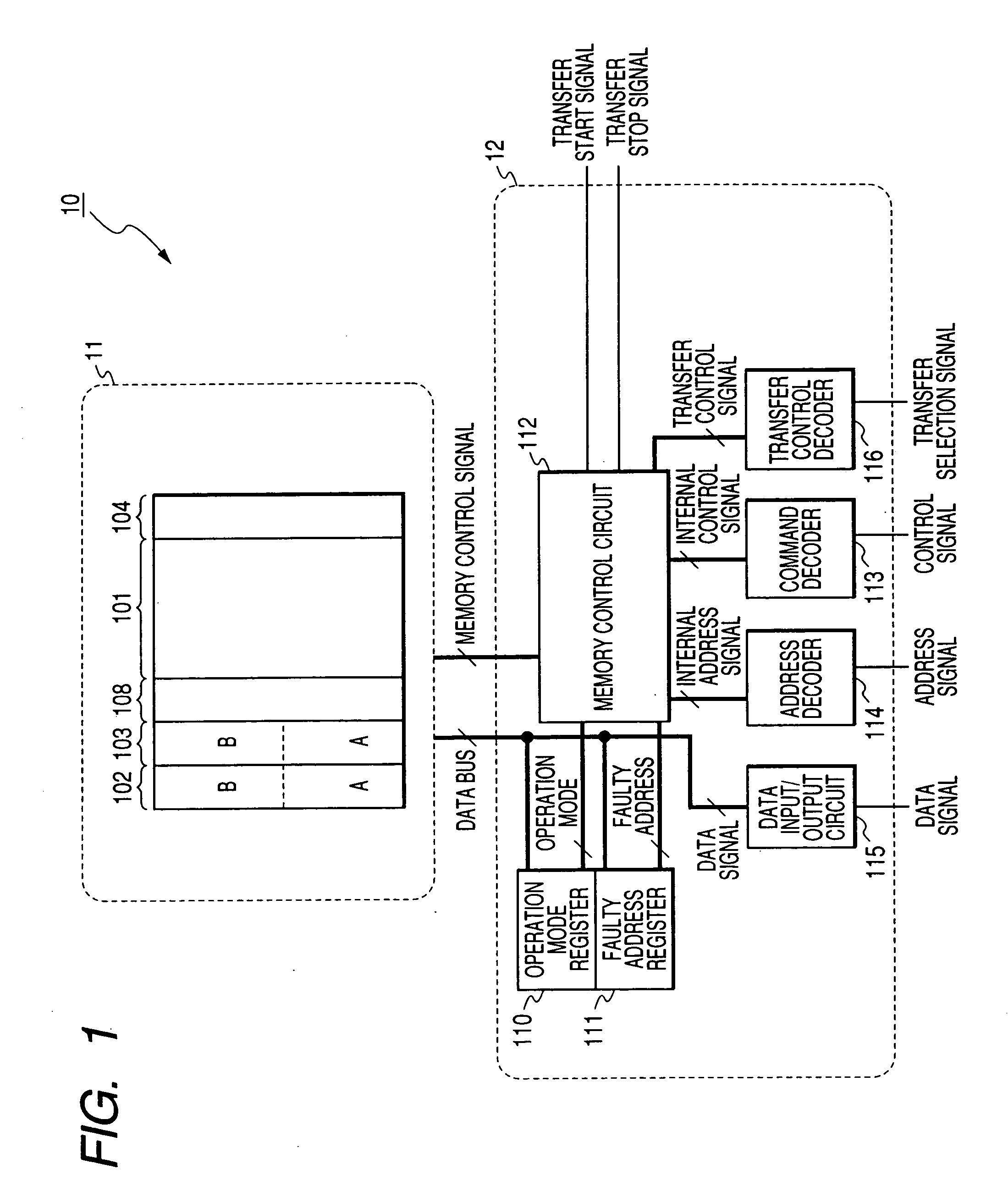
[0061]FIG. 1 is a block diagram showing the configuration of a semiconductor storage device 10 according to a first embodiment of the present invention; that is, a configuration using a physical fuse and ferroelectric memory (FeRAM) as nonvolatile memory.

[0062] As shown in FIG. 1, the semiconductor storage device 10 is made up of a memory cell array section 11 formed from nonvolatile memory, and a peripheral circuit section 12 for enabling input / output of data into / from the memory cell array section 11 and memory control.

[0063] The memory cell array section 11 is made up of a physical fuse and ferroelectric memory, and individual sections of the configuration will be described below.

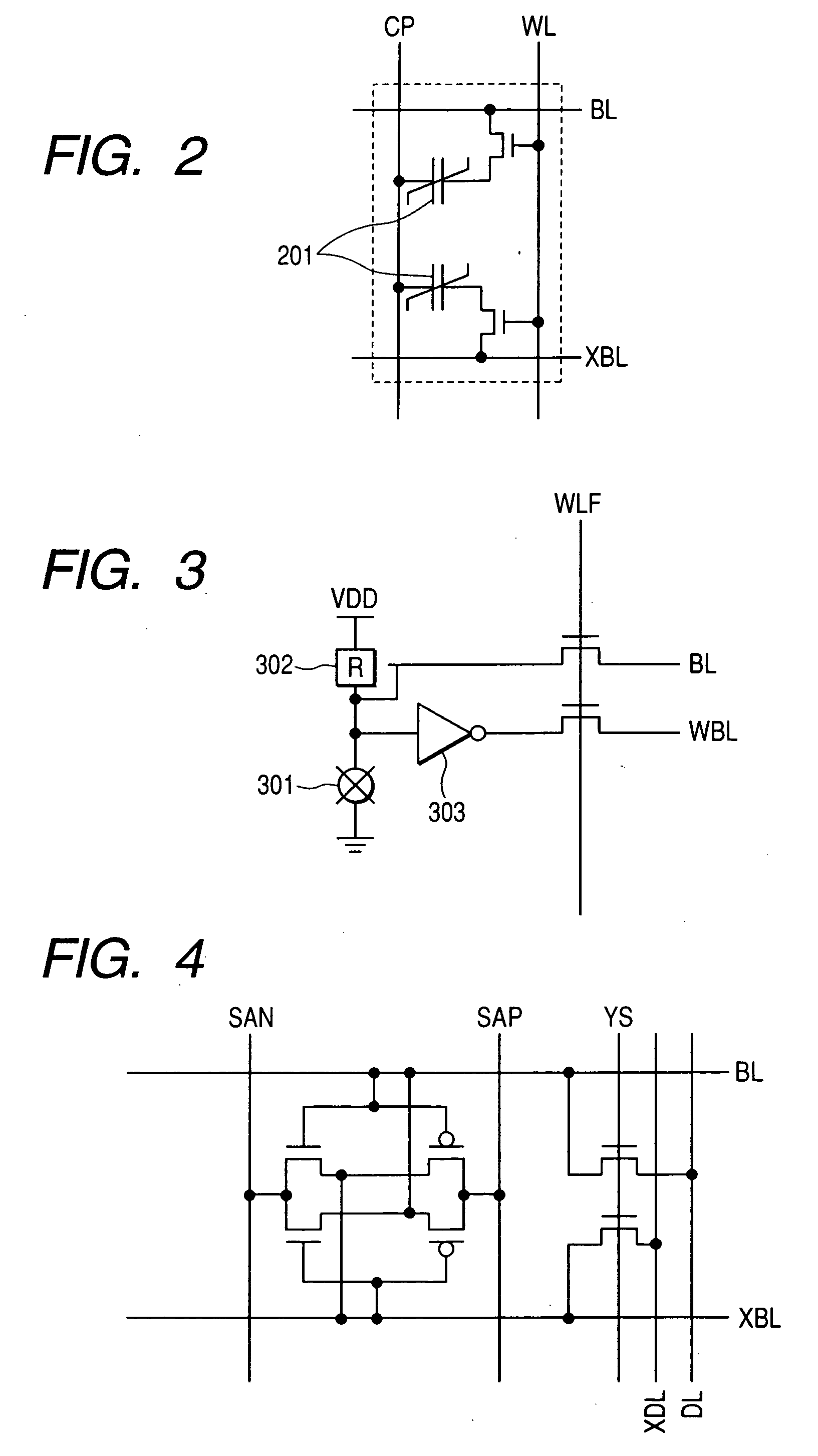
[0064] Reference numeral 101 designates a main storage area for storing ordinary data which is formed from a 2T2C ferroelectric memory cell shown in FIG. 2. Reference numeral 108 designates a redundant storage area for storing information in lieu of a faulty area (a deficient memory cell) of the main ...

second embodiment

[0101]FIG. 8 is a block diagram showing the configuration of a semiconductor storage device 20 according to a second embodiment of the present invention; that is, a configuration using a physical fuse and ferroelectric memory (FeRAM) as nonvolatile memory.

[0102] As shown in FIG. 8, the semiconductor storage device 20 is made up of a memory cell array section 21 formed from nonvolatile memory, and a peripheral circuit section 22 for enabling input / output of data into / from the memory cell array section 21 and memory control.

[0103] The memory cell array section 21 is made up of a physical fuse and ferroelectric memory, and individual sections of the configuration will be described below.

[0104] Reference numeral 701 designates a main storage area for storing ordinary data which is formed from the 2T2C ferroelectric memory cell, as in the case of the first embodiment (see FIG. 2). Reference numeral 708 designates a redundant storage area for storing information in lieu of a faulty are...

third embodiment

[0138]FIG. 12 is a block diagram showing the configuration of a semiconductor storage device 30 according to a third embodiment of the present invention; that is, a configuration using a physical fuse and ferroelectric memory (FeRAM) as nonvolatile memory.

[0139] As shown in FIG. 12, the semiconductor storage device 30 is made up of a memory cell array section 31 formed from nonvolatile memory, and a peripheral circuit section 32 for enabling input / output of data into / from the memory cell array section 31 and memory control.

[0140] The memory cell array section 31 is made up of a physical fuse and ferroelectric memory, and individual sections of the configuration will be described below.

[0141] Reference numeral 901 designates a main storage area for storing ordinary data which is formed from the 2T2C ferroelectric memory cell, as in the case of the first embodiment (see FIG. 2). Reference numeral 908 designates a redundant storage area for storing information in lieu of a faulty ar...


PUM


Abstract

To provide a semiconductor storage device which can adapt to assembly processes involving different treatment temperatures, can become unrewritable when rewriting of data by the user is prohibited, negates the necessity for developing different semiconductor storage devices, and lowers development cost. A semiconductor storage device is provided with, as areas for storing faulty address information indicating a faulty area and operation mode setting information about the semiconductor storage device, a first setting function storage area 103 formed from electrically-rewritable nonvolatile memory and a second setting function storage area 102 formed from once-rewritable nonvolatile memory. Transfer of faulty address information to a faulty address register 111 and transfer of operation mode setting information to an operation mode register 110 are selectively performed.

Description

BACKGROUND OF THE INVENTION [0001] 1. Filed of the Invention [0002] The present invention relates to a semiconductor storage device including nonvolatile memory, and more particularly, to a semiconductor storage device including nonvolatile memory for storing address information about a faulty area, memory operation setting information, and operation setting information about a semiconductor storage device, or the like. [0003] 2. Description of the Related Art [0004] Recently, nonvolatile memory having the function of latching data even at power-off includes flash memory, electrically-rewritable nonvolatile semiconductor memory (EEPROM or the like), and ferroelectric memory (FeRAM). [0005] Such nonvolatile memory can be optimized by storing operation modes of the semiconductor storage device in which the memory is contained. When a deficiency is found in a memory cell, the address of the faulty area is stored, and the information is utilized, thereby replacing the memory cell in the...

Claims


Application Information

Patent Timeline
Patent Type & Authority Applications(United States)
IPC IPC(8): G11C11/22G11C7/00G11C29/00G11C29/12
CPCG11C11/22G11C2029/4402G11C29/816G11C29/789
Inventor MURAKUKI, YASUOHIRANO, HIROSHIGEGOHOU, YASUSHISAKAGAMI, MASAHIKOYAMAOKA, KUNISATOIWANARI, SHUNICHINAKAKUMA, TETSUJIMIKI, TAKASHI
Owner PANASONIC CORP
Learn More