

IC tiling pattern method, IC so formed and analysis method
a technology of fill tile pattern and fill tile pattern, which is applied in the direction of cad circuit design, program control, instruments, etc., can solve the problems of inability to make consistent assumptions about the impact of fill tile pattern on electrical properties, fill tile pattern complexity, and inability to add fill tile to the electrical analysis of the circui
- Summary
- Abstract
- Description
- Claims
- Application Information
AI Technical Summary
Benefits of technology
Problems solved by technology
Method used
Image

Examples
Embodiment Construction
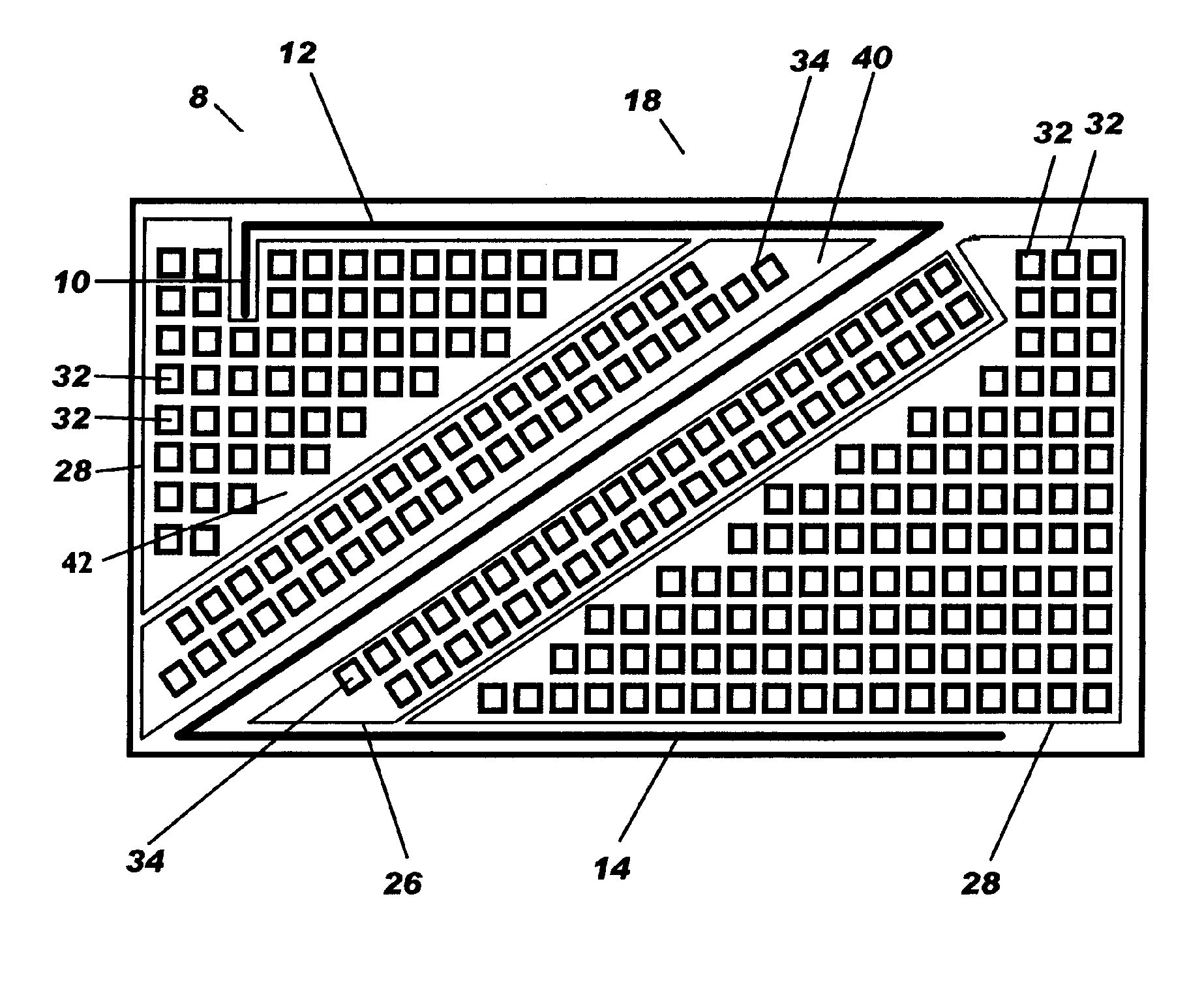
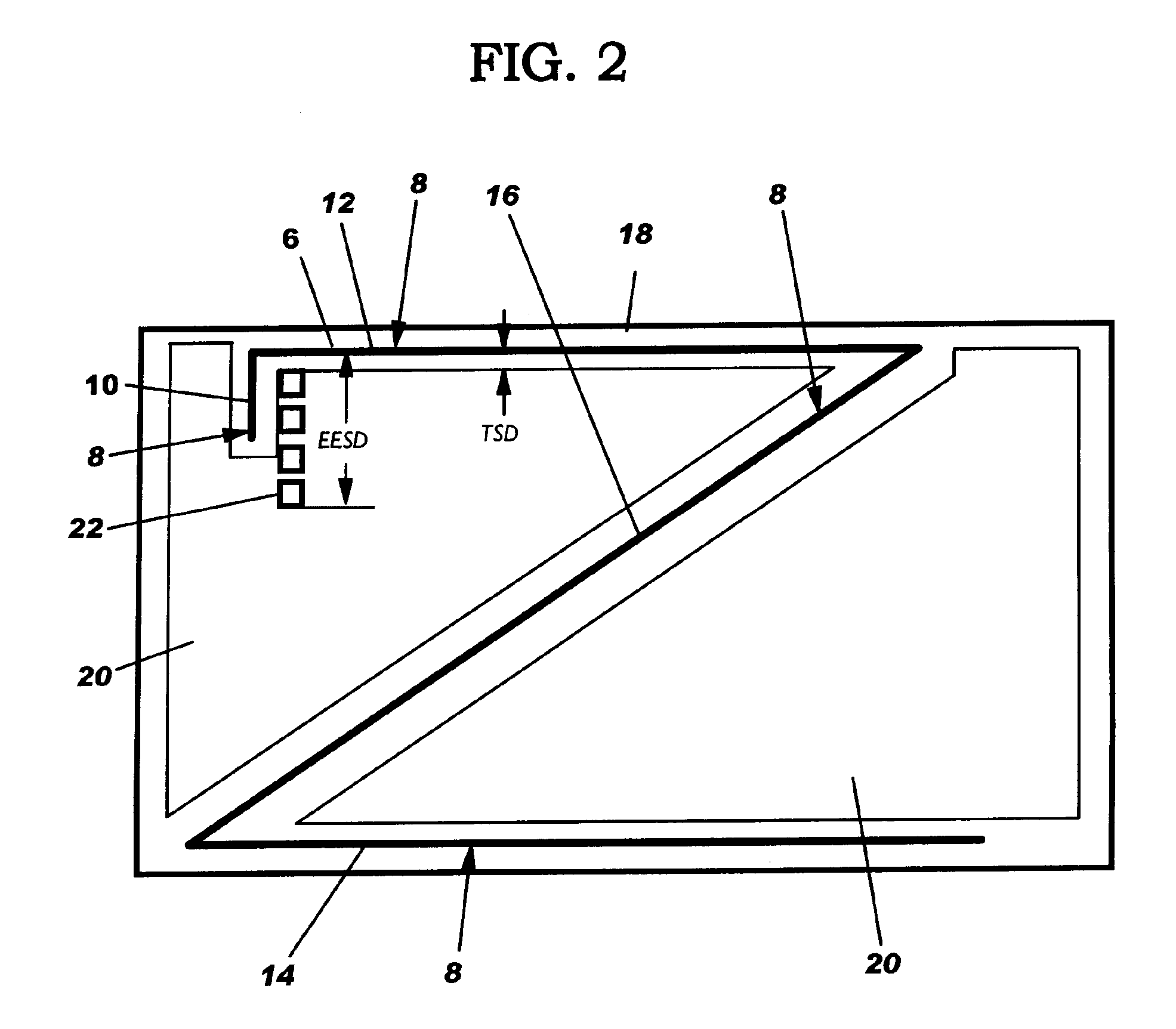
[0015] With reference to the accompanying drawings, FIG. 2 shows a layer of an integrated circuit (IC) 6 including, among other things, a number of electrically impressionable parts 8. By “impressionable” is meant that the parts are susceptible to environmental influences that can alter their electrical properties. Hereinafter, electrically impressionable parts 8 will be described as wire segments 10, 12, 14, 16. It should be recognized, however, that a part 8 may be any structure of IC 6 that is electrically impressionable such as a resistor, well, power bus segment, shielding structure, ground plane, wave guide, etc. In one embodiment, wire segments 10, 12, 14 may be considered orthogonal because of their relation to each other and / or other structure of IC 6 (e.g., a “top” surface 18), and segment 16 may be considered non-orthogonal because of its relation to segments 10, 12, 14 or other structure of IC 6. It should be recognized that while a particular structural (i.e., wiring) p...
PUM
 Abstract
Description
Claims
Application Information