Novel semiconductor device design

Inactive Publication Date: 2005-12-15
TAIWAN SEMICON MFG CO LTD
View PDF35 Cites 23 Cited by
  • Summary
  • Abstract
  • Description
  • Claims
  • Application Information

AI Technical Summary

Benefits of technology

[0007] In accordance with one aspect of the present invention, a slant contact is formed by shifting a portion of a contact a distance less than a whole dimension of the contact along the direction shifted. The slant contact typically has an oval shape due to optical and etching effects. With slant contacts, the optical proximity effect is reduced or eliminated. Using slant contacts increases the device density in an integrated circuit and reduces cross talk.
[0008] In accordance with another aspect of the present invention, a six-transistor SRAM cell is designed using a compound interconnection having a doped semiconductor covered with a silicide. The compound interconnection interconnects a source of a pass gate transistor, a drain of a pull down tran

Problems solved by technology

However, problems arise when elements are so close that optical proximity effects occur.
However,

Method used


Image

  • Novel semiconductor device design
  • Novel semiconductor device design
  • Novel semiconductor device design

Examples


Embodiment Construction

[0022] The making and using of the presently preferred embodiments are discussed in detail below. It should be appreciated, however, that the present invention provides many applicable inventive concepts that can be embodied in a wide variety of specific contexts. The specific embodiments discussed are merely illustrative of specific ways to make and use the invention, and do not limit the scope of the invention.

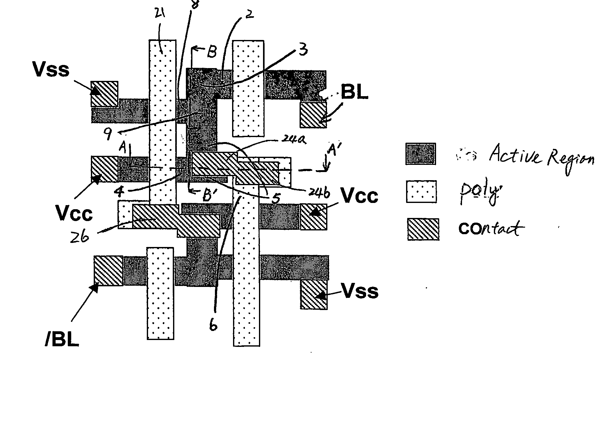
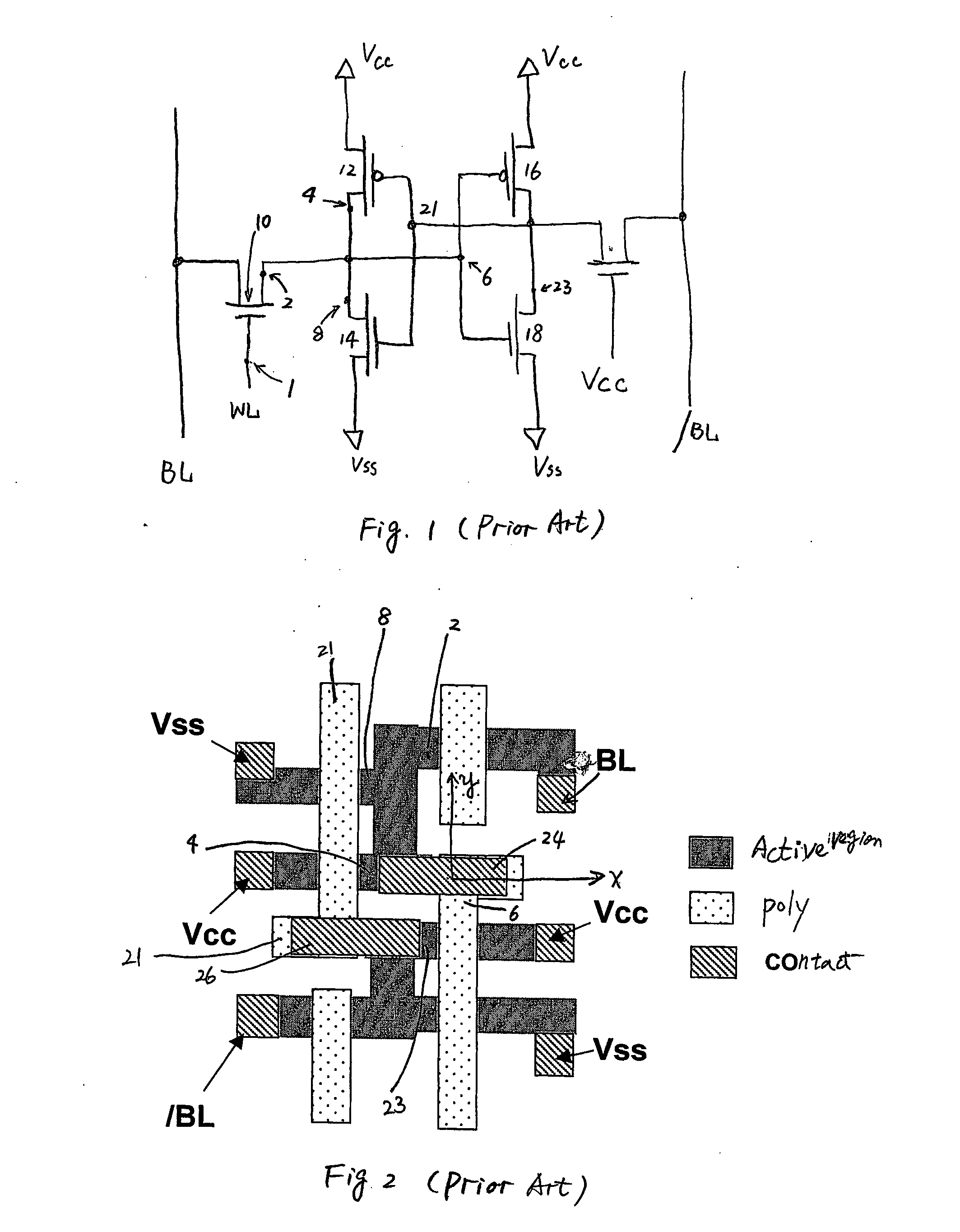
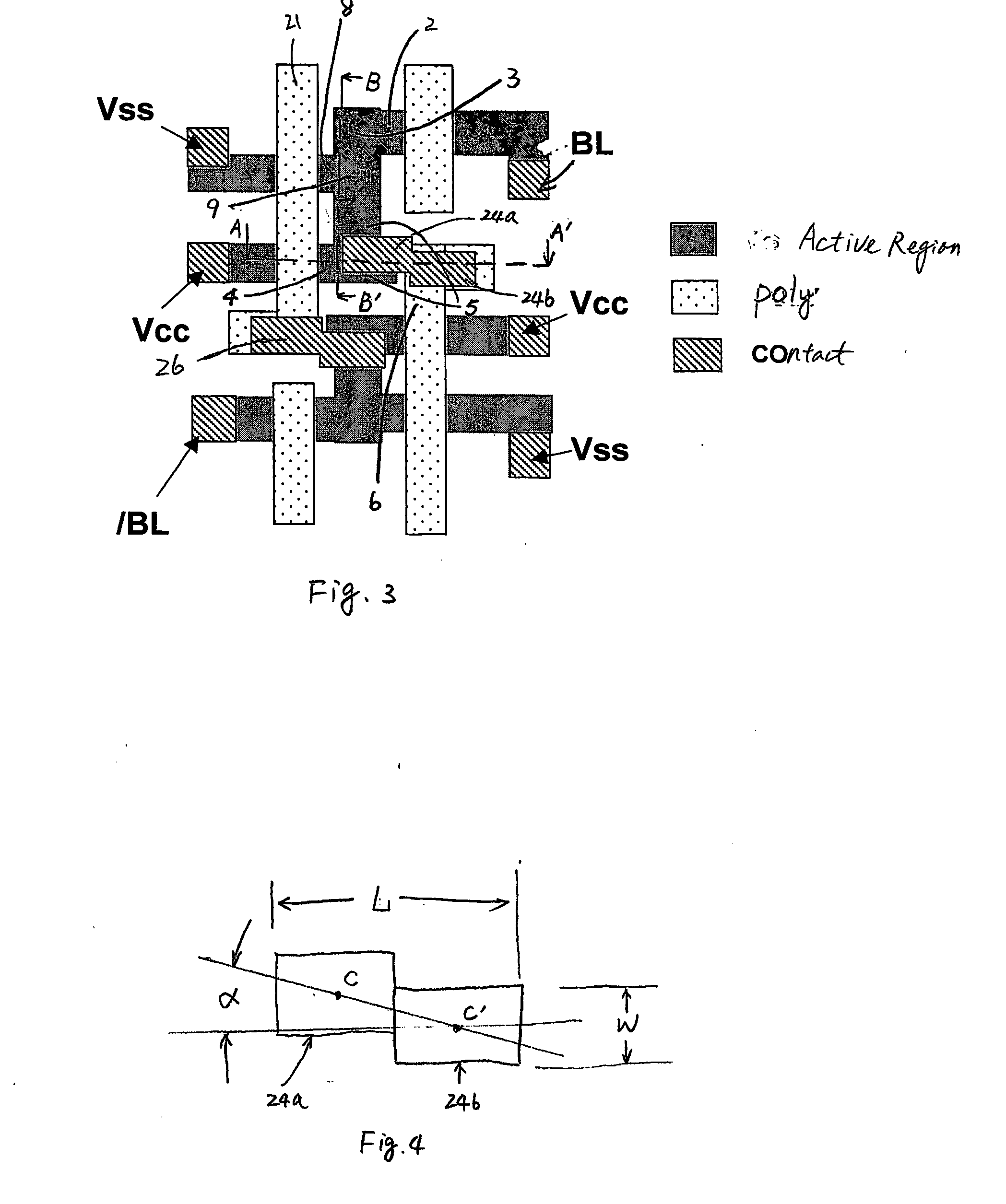
[0023] Typically, layouts are made along grids or reticles having two directions vertical to each other, namely, x and y directions. In order to reduce the optical proximity between neighboring contacts, the contacts have to be sufficiently separated. It is preferred that the contacts are evenly distributed to make better use of the layout area. However, it is hard to place a long contact without incurring excessive loss of layout space. This is especially true for the layout of SRAM cells due to the high density of the memory chip. The preferred embodiments of the present ...


PUM


Abstract

An integrated circuit having small layout area and a method of forming the same are provided. A slant contact is formed by shifting a portion of a contact a distance less than a whole dimension of the contact along the direction shifted. By using slant contacts, the optical proximity effect is reduced, the device density in the integrated circuit is increased and cross talk is reduced. In the preferred embodiment, the slant contact is combined with other techniques such as compound interconnection, butted local interconnection and slim spacers to reduce the layout area. In another embodiments, a six-transistor SRAM cell can be designed with a slant contact, compound interconnection and butted local interconnection to reduce the layout area.

Description

[0001] This application claims the benefit of U.S. Provisional Application No. 60 / 578,726, filed on Jun. 10, 2004, entitled “SRAM Cell Design,” and further claims the benefit of U.S. Provisional Application No. 60 / 582,931, filed on Jun. 25, 2004, entitled “SRAM Cell Design,” which applications are hereby incorporated herein by reference.TECHNICAL FIELD [0002] This invention relates generally to semiconductor devices, and specifically to the design of semiconductor devices having small layout areas. BACKGROUND [0003] With the scaling of VLSI circuits, more devices are put into a single chip. This not only requires the shrinking of device size, but it also requires the improvement of layout techniques. [0004] One example is static random access memory (SRAM). Due to the high capacity requirement of the memory, being able to reduce the layout area is especially important. The elements of the devices are laid out closely to save space. However, problems arise when elements are so close ...

Claims


Application Information

Patent Timeline
IPC IPC(8): H01L21/768H01L27/02H01L29/76
CPCH01L21/76838H01L21/76895H01L27/0207
Inventor HUANG, CHIEN-CHAOCHEN, HAO-YUYANG, FU-LIANGHUANG, CHENG-CHUANCHUNG, TONG-HEUAN
Owner TAIWAN SEMICON MFG CO LTD
Why Eureka
Try Eureka