RAISED STI PROCESS FOR MULTIPLE GATE OX AND SIDEWALL PROTECTION ON STRAINED Si/SGOI STRUCTURE WITH ELEVATED SOURCE/DRAIN

a technology of strained si/sgoi and gate ox, which is applied in the direction of semiconductor devices, single crystal growth, chemistry apparatus and processes, etc., can solve the problem of short circuit with a neighboring active area, and achieve the effect of reducing unnecessary poly over etching, and reducing the number of sidewalls

Inactive Publication Date: 2005-12-15
GLOBALFOUNDRIES INC
View PDF86 Cites 352 Cited by
  • Summary
  • Abstract
  • Description
  • Claims
  • Application Information

AI Technical Summary

Benefits of technology

[0013] In the present invention, the gate formation process can be done without any restriction of oxide removal. Hence, items (A), (B) and (E) mentioned above are resolved. Moreover, the gate polySi top surface is planarized in the present invention by a two step gate poly deposition (before and after trench isolation) thereby eliminating unnecessary poly over etching. Also, the inventive structure allows for a higher trench isolation height as compared to the conventional process. Hence, the present invention resolves the issues mentioned under items (C)-(D) above. Furthermore, due to the higher trench isolation height that can be achieved in the present invention, a disposable nitride spacer can be employed which protects the sidewalls of the strained Si thereby resulting in little or no Si loss at the isolation trench edge.

Problems solved by technology

In the prior art process, an oxide divot is typically formed in the strained Si / SGOI structure, which can result in a short circuit with a neighboring active area when a polySi stringer is present in the divot.

Method used


Image

  • RAISED STI PROCESS FOR MULTIPLE GATE OX AND SIDEWALL PROTECTION ON STRAINED Si/SGOI STRUCTURE WITH ELEVATED SOURCE/DRAIN
  • RAISED STI PROCESS FOR MULTIPLE GATE OX AND SIDEWALL PROTECTION ON STRAINED Si/SGOI STRUCTURE WITH ELEVATED SOURCE/DRAIN
  • RAISED STI PROCESS FOR MULTIPLE GATE OX AND SIDEWALL PROTECTION ON STRAINED Si/SGOI STRUCTURE WITH ELEVATED SOURCE/DRAIN

Examples


Embodiment Construction

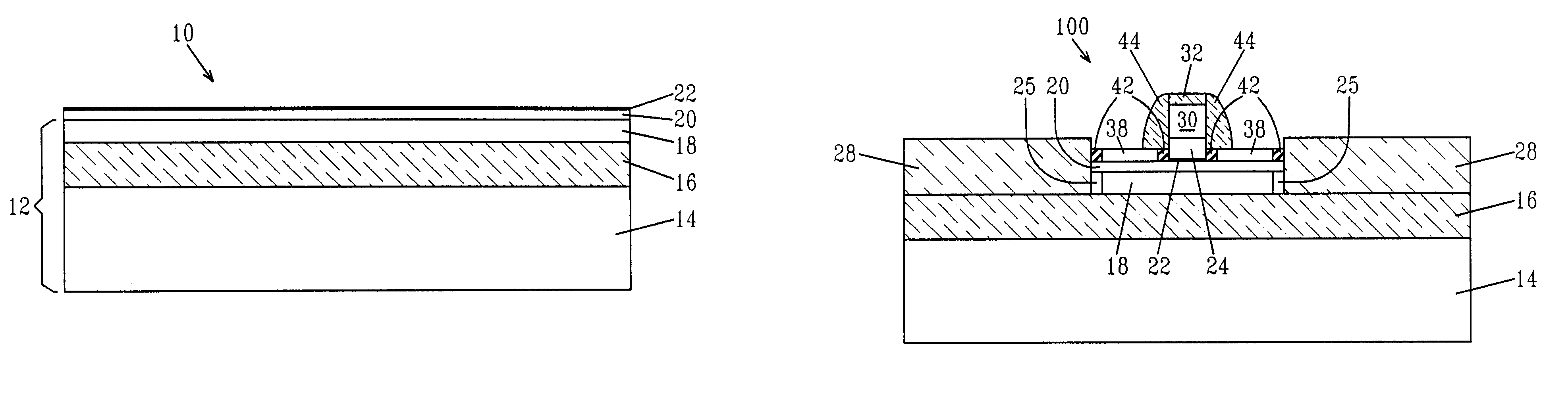
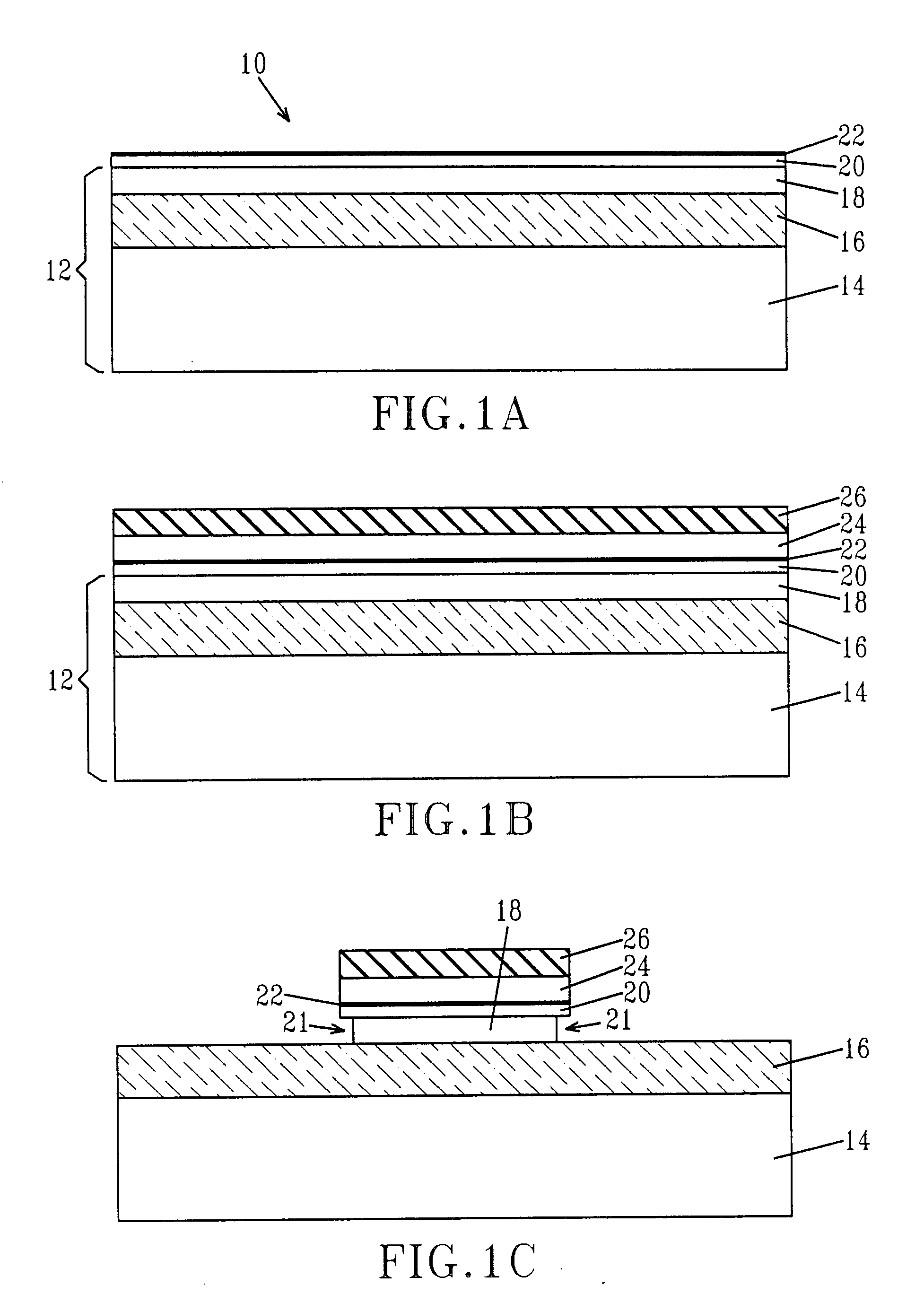
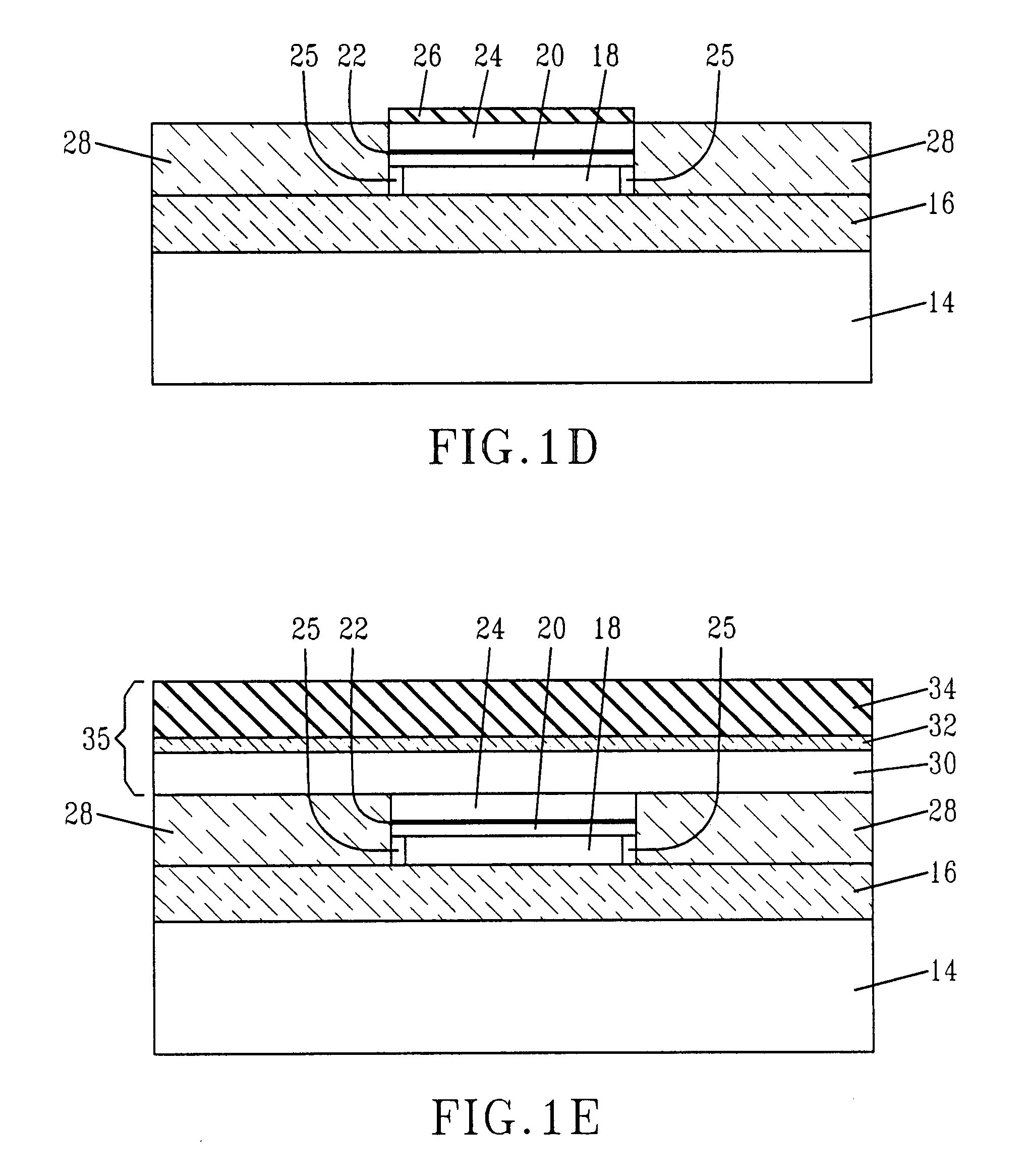
[0028] The present invention, which provides a strained Si / SGOI structure having an elevated source / drain region and a raised trench isolation region and a method of fabricating the same, will now be described in greater detail by referring to drawings that accompany the present application.

[0029] Reference is first made to FIG. 1A, which illustrates an initial structure 10 that is employed in the present invention. The initial structure 10 comprises a SiGe-on-insulator (SGOI) substrate 12, a strained Si layer 20 located on a surface of the SGOI substrate 12, and a gate dielectric 22 located on a surface of the strained Si layer 20. As shown, the SGOI substrate 12 includes a Si-containing substrate layer 14, an insulating layer 16, and a SiGe layer 18 that is in a relaxed state.

[0030] The SGOI substrate 12 can be fabricated using any conventional process in which a relaxed SiGe layer is formed atop a surface of an insulating layer. In one embodiment, for example, the SGOI substrat...


PUM

PropertyMeasurementUnit
thicknessaaaaaaaaaa
thicknessaaaaaaaaaa
thicknessaaaaaaaaaa

Abstract

The present invention provides a strained / SGOI structure that includes an active device region of a relaxed SiGe layer, a strained Si layer located atop the relaxed SiGe layer, a raised source / drain region located atop a portion of the strained Si layer, and a stack comprising at least a gate dielectric and a gate polySi located on another portion of the strained Si layer; and a raised trench oxide region surrounding the active device region. The present invention also provides a method of forming such a structure. In the inventive method, the gate dielectric is formed prior to trench isolation formation thereby avoiding many of the problems associated with prior art processes in which the trench oxide is formed prior to gate dielectric formation.

Description

BACKGROUND OF INVENTION [0001] The present invention relates to semiconductor devices, and more particularly to a strained Si / silicon germanium-on-insulator (SGOI) structure having an elevated source / drain region and a raised trench isolation region. The present invention also relates to a method of fabricating such a strained Si / SGOI structure. [0002] Improvements in transport properties, i.e., carrier mobility, through strain have been demonstrated in the operating characteristics of field effect transistors (FETs). For complementary metal oxide semiconductor (CMOS) devices, an improvement in device characteristics through carrier mobility has significant potential for the fabrication of very high-speed devices. Strained silicon on a relaxed SiGe substrate is one system where such an improvement occurs. [0003] Experimental research on enhanced carrier mobility MOSFETs caused by strain has concentrated on a strained Si layer grown on a relaxed SiGe layer that is located on a bulk s...

Claims


Application Information

Patent Timeline
Patent Type & Authority Applications(United States)
IPC IPC(8): C30B1/00H01L21/20H01L21/336H01L21/36H01L21/762H01L29/10H01L29/51H01L29/786
CPCH01L21/76243H01L21/76251H01L29/1054H01L29/41783H01L29/516Y10S438/938H01L29/6653H01L29/66628H01L29/66742H01L29/7842H01L29/78687H01L29/517
Inventor BEINTNER, JOCHENBRONNER, GARY B.DIVAKARUNI, RAMACHANDRAKIM, BYEONG Y.
Owner GLOBALFOUNDRIES INC
Why Eureka
Try Eureka