
Semiconductor light emitting device and semiconductor light emitting unit

a light-emitting device and semiconductor technology, applied in the direction of semiconductor devices, basic electric elements, electrical appliances, etc., can solve the problems of increasing assembly costs, increasing assembly costs, and increasing the number of components,

Inactive Publication Date: 2005-12-22
KK TOSHIBA
View PDF6 Cites 223 Cited by
  • Summary
  • Abstract
  • Description
  • Claims
  • Application Information

AI Technical Summary

Problems solved by technology

Thermal resistance of the adhesive layer has not been sufficiently reduced.
Many assembly steps are involved, which increases assembly cost.
The cost rises due to increase in the number of components (heat sink, lead frame, adhesive, etc.).
Additionally, a semiconductor light emitting device with a lead frame having higher thermal conductivity for driving an LED at high current suffers large thermal stress in the solder reflow process.
For this reason, use of a less heat-resistant adhesive such as silver paste for mounting the LED may cause degradation in reliability including degradation in adhesion strength.
However, conventional SMDs have another problem that it is difficult to mount the LED using eutectic solder because resin for molding the inner lead section of a lead frame has a low heat resistance temperature.

Method used


Image

  • Semiconductor light emitting device and semiconductor light emitting unit
  • Semiconductor light emitting device and semiconductor light emitting unit
  • Semiconductor light emitting device and semiconductor light emitting unit

Examples


Embodiment Construction

[0045] Embodiments of the invention will now be described with reference to the drawings.

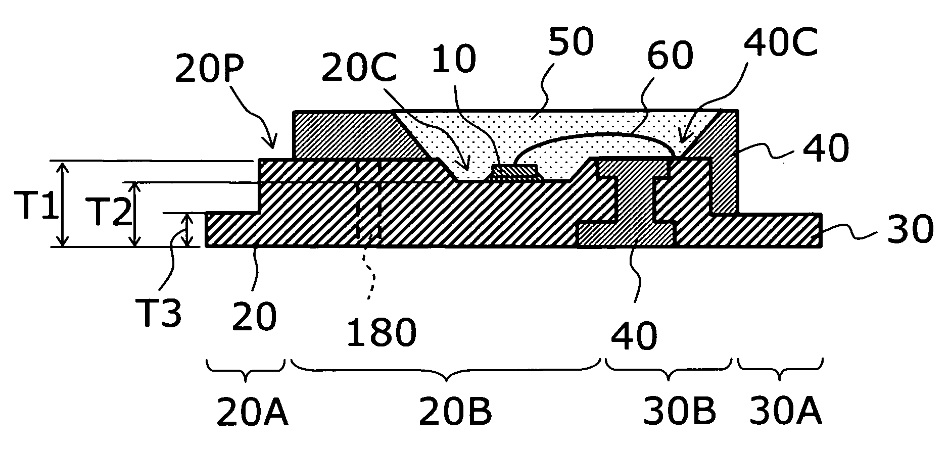
[0046]FIG. 1 is a schematic cross-sectional view illustrating the configuration of the relevant part of a semiconductor light emitting device according to an embodiment of the invention.

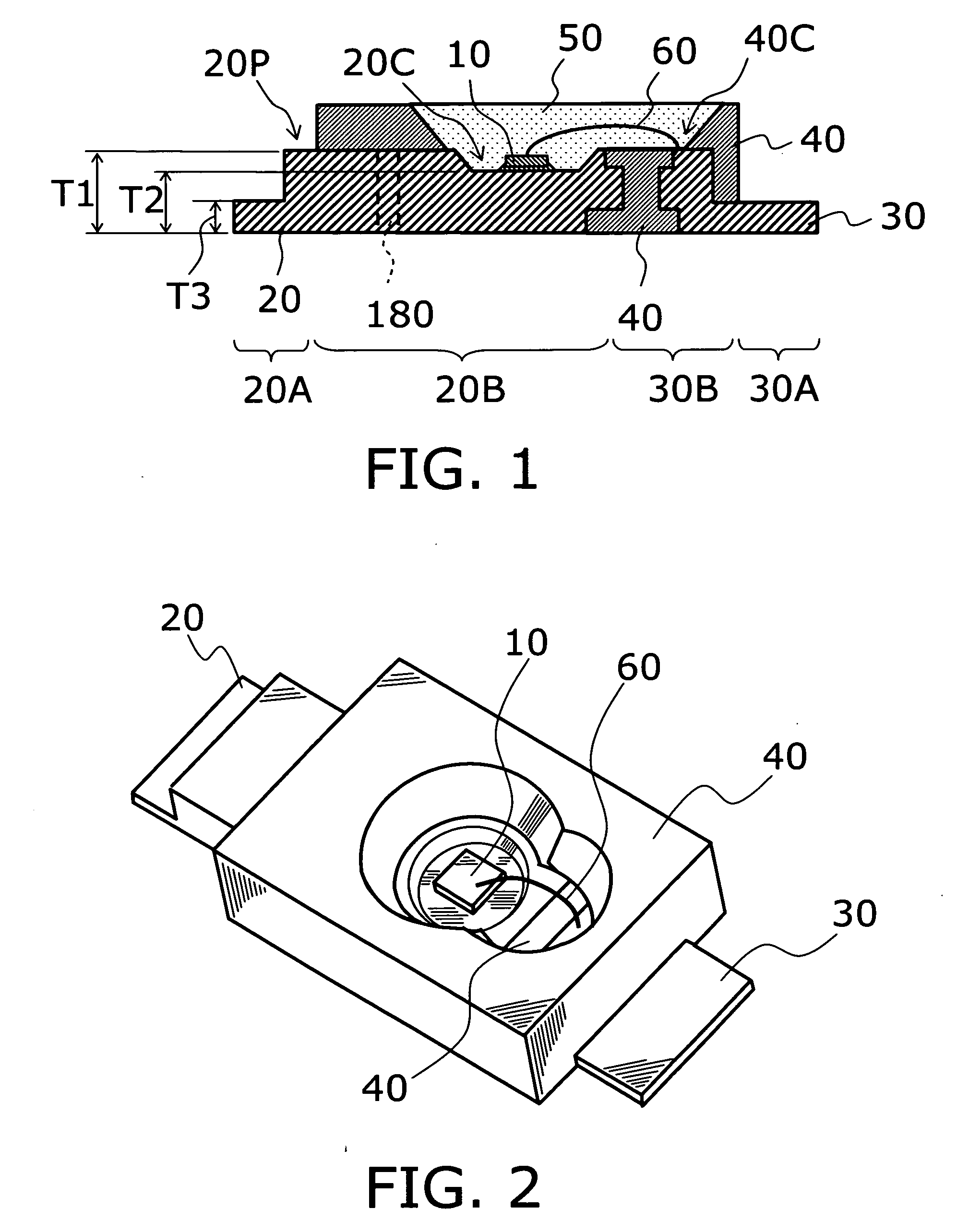
[0047]FIG. 2 is a schematic perspective view of the semiconductor light emitting device as viewed obliquely from above.

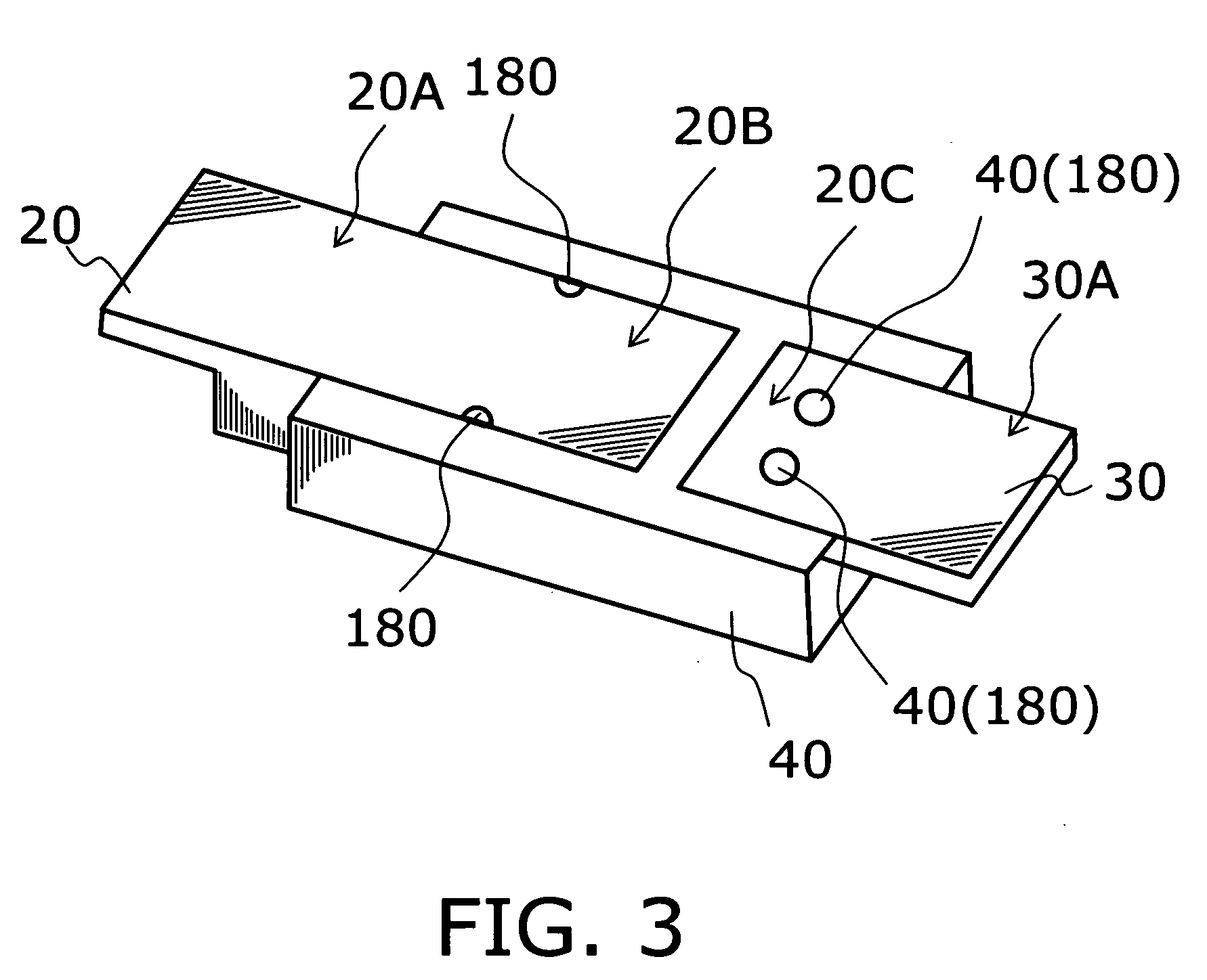
[0048]FIG. 3 is a schematic perspective view of the semiconductor light emitting device as viewed obliquely from below.

[0049] More specifically, the semiconductor light emitting device of this embodiment, which is a light emitting device of the so-called surface mount device (SMD) type, comprises a pair of leads 20 and 30, and embedding resin 40 formed to encompass inner lead sections 20B and 30B of the leads 20 and 30. A semiconductor light emitting chip 10 (hereinafter referred to as “LED chip”) is mounted on the lead 20. This semiconductor light emitting device can be mounted, for example,...


PUM


Abstract

A semiconductor light emitting device comprises: embedding resin; a first lead having a first inner lead section embedded in the embedding resin and a first outer lead section protruding from one side face of the embedding resin; a second lead having a second inner lead section embedded in the embedding resin and a second outer lead section protruding from a side face opposed to the one side face of the embedding resin; a semiconductor light emitting chip mounted on a portion of the first inner lead section exposed in a recess provided on an upper face of the embedding resin; and a wire connecting the semiconductor light emitting chip with the second lead. The first and second inner lead sections and the first and second outer lead sections each have a substantially coplanar rear face. At least a part of the rear face of the first inner lead section and at least a part of the rear face of the second inner lead section are not covered with the embedding resin but are exposed.

Description

CROSS-REFERENCE TO RELATED APPLICATIONS [0001] This application is based upon and claims the benefit of priority from the prior Japanese Patent Application No. 2004-174455, filed on Jun. 11, 2004; the entire contents of which are incorporated herein by reference. BACKGROUND OF THE INVENTION [0002] This invention relates to a semiconductor light emitting device and a semiconductor light emitting unit, and more particularly to a semiconductor light emitting device suitable to applications requiring high current drive such as backlights for liquid crystal displays and high power LED (light emitting diode) lamps, and a semiconductor light emitting unit with this semiconductor light emitting device being mounted. [0003] In recent years, LEDs, among other semiconductor light emitting devices, have shown a remarkable progress in technology, including white light emitting LEDs using ultraviolet excitation of phosphors. Light emission of every display color on the CIE (International Commissi...

Claims


Application Information

Patent Timeline
IPC IPC(8): H01L29/22H01L33/56H01L33/60H01L33/62H01L33/64
CPCH01L33/486H01L2224/49109H01L33/642H01L33/647H01L2224/48091H01L2224/48247H01L2224/48257H01L2224/73265H01L2224/92247H01L2924/01046H01L2924/01078H01L2924/01079H01L33/62H01L2224/97H01L24/97H01L2224/32257H01L2924/01019H01L2924/01322H01L2224/32245H01L2924/12041H01L2924/00014H01L2924/00012H01L2924/00H01L2924/351H01L2924/181H01L24/73
Inventor OSHIO, HIROAKIMATSUMOTO, IWAOMIYAKAWA, TAKESHITAKEZAWA, HATSUO
Owner KK TOSHIBA
Features
  • Generate Ideas
  • Intellectual Property
  • Life Sciences
  • Materials
  • Tech Scout
  • Unparalleled Data Quality
  • Higher Quality Content
  • 60% Fewer Hallucinations
Learn More