Probe card and the production method

a technology of probe card and production method, applied in the field of probe card, can solve problems such as contact errors, and achieve the effect of low processing accuracy of substrate and high precision in needle position

Active Publication Date: 2005-12-22
ADVANTEST CORP
View PDF3 Cites 27 Cited by
  • Summary
  • Abstract
  • Description
  • Claims
  • Application Information

AI Technical Summary

Benefits of technology

[0020] Generally, processing accuracy of the substrate is lower comparing with that of the probe guide and positions of holes formed in the substrate, etc. are not always precise, but according to the above inventions (inventions 5 and 6), the substrate-side probe guide can be fixed to the substrate a

Problems solved by technology

The larger a probe area on the probe card is, the larger the positional deviation becomes, which c

Method used


Image

  • Probe card and the production method
  • Probe card and the production method
  • Probe card and the production method

Examples


Embodiment Construction

[0027] Below, a probe card according to an embodiment of the present invention will be explained based on the drawings.

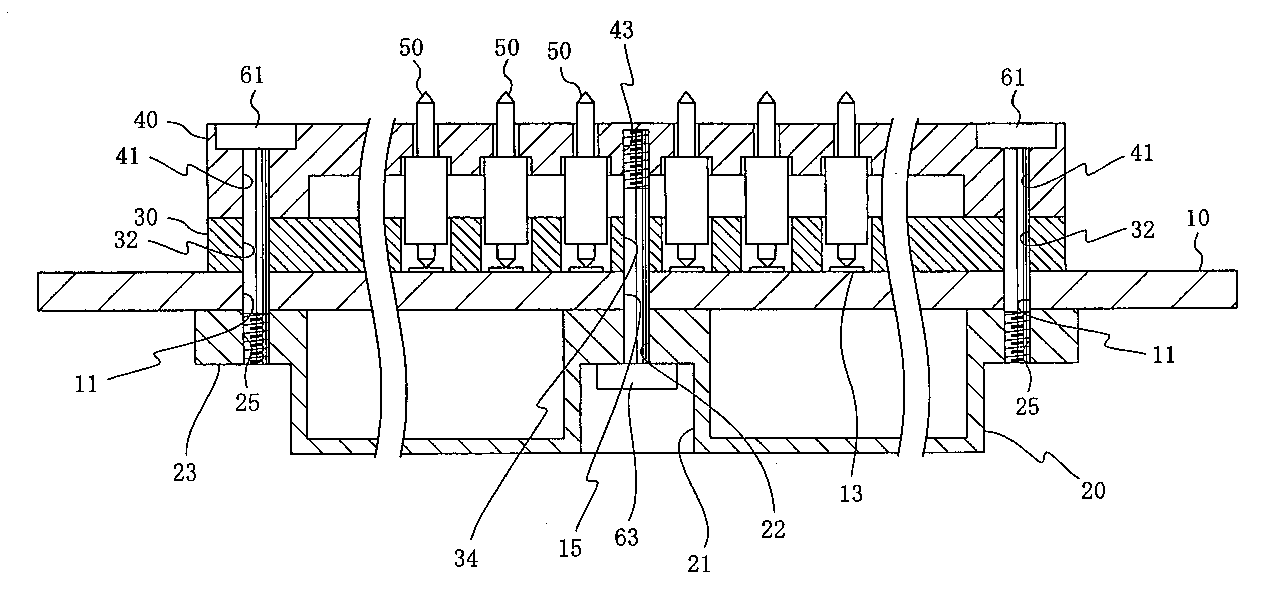
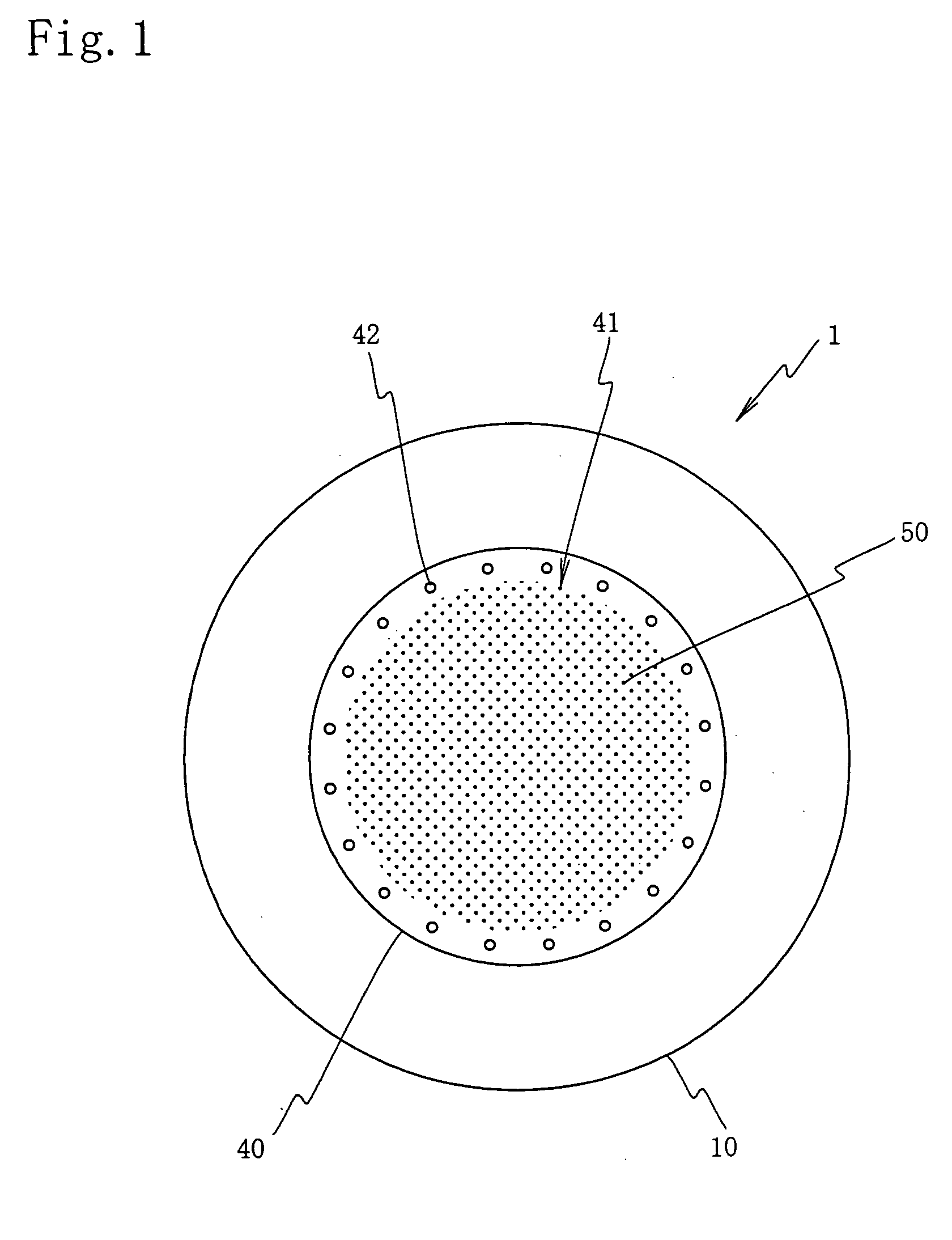
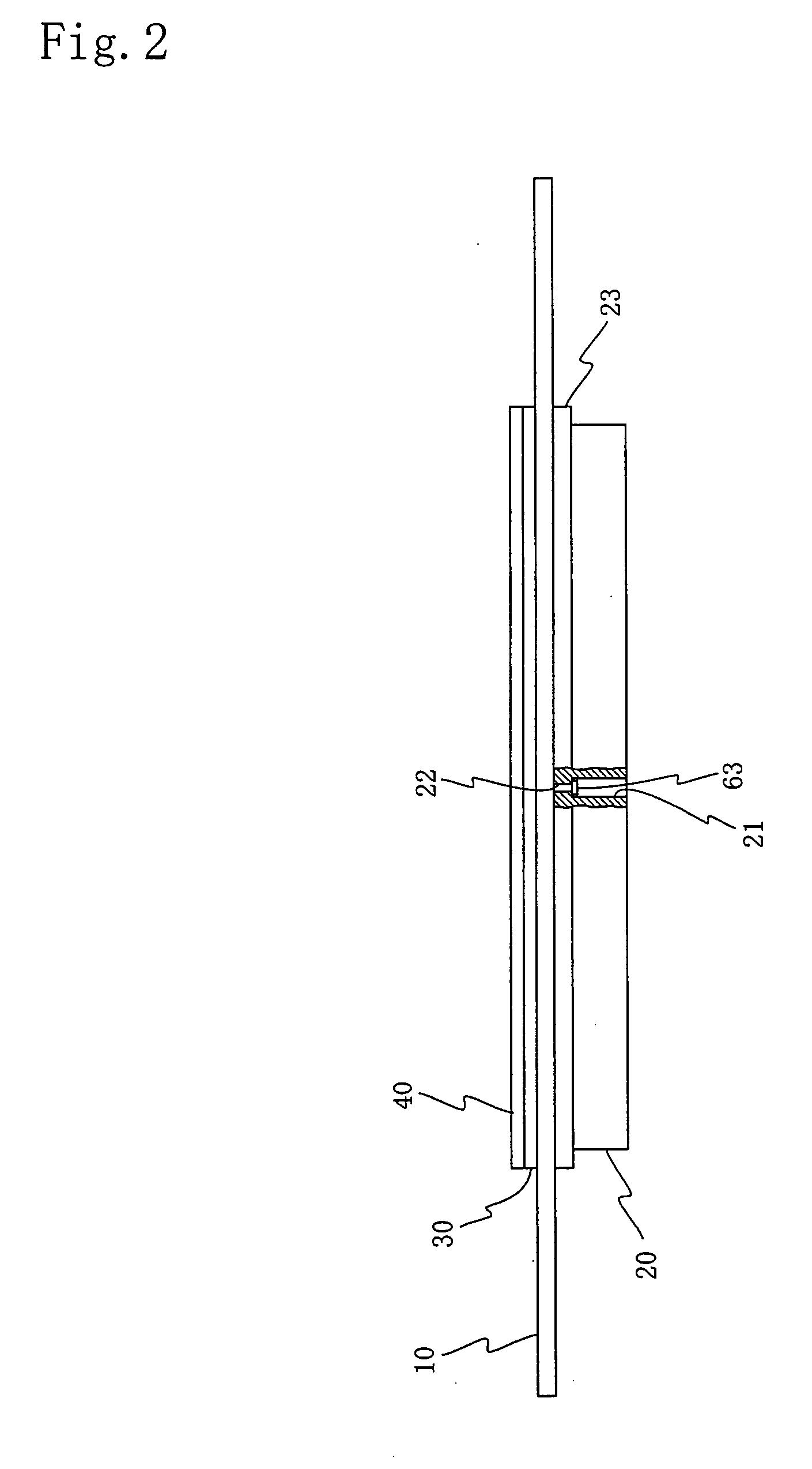
[0028] A probe card 1 according to the present embodiment is, as shown in FIG. 1 to FIG. 5, configured by including a print substrate 10, a stiffener 20 provided on the test head side of the print substrate 10, two probe guides 30 and 40 provided one above the other on the opposite side of the test head of the print substrate 10, and a plurality of probe pins 50 supported by the probe guides 30 and 40.

[0029] The probe guide 30 is directly arranged on a surface (front surface) on the opposite side of the test head on the print substrate 10 and composes a substrate-side probe guide (hereinafter, “a probe guide 30” will be also referred to as “a substrate-side probe guide 30”). Also, the probe guide 40 is stacked and fixed on the probe guide 30 and composes a wafer-side probe guide (hereinafter, “a probe guide 40” will be also referred to as “a wafer-side probe guide...


PUM


Abstract

A probe card 1 is composed of a plurality of probe pins 50 having wafer-side plungers 51 at one end portion and substrate-side plungers 52 on the other end side; two probe guides 30 and 40 one above the other for supporting the plurality of probe pins 50, so that the plurality of probe pins 50 are arranged to be corresponding to an arrangement of external terminals of a semiconductor wafer and the wafer-side plungers 51 of the probe pins 50 protrude; a print substrate 10 having pads 13 for the substrate-side plungers 52 of the probe pins 50 supported by the probe guides 30 and 40 to contact; and a stiffener 20 provided on the back surface of the print substrate 10. The probe guides 30 and 40 are produced by a material having substantially the same thermal expansion coefficient as that of the semiconductor wafer, and fixed to the print substrate 10 and the stiffener 20 at the circumferential portion and the center portion.
The probe card 1 configured as above is capable of maintaining high precision in needle positions of the probe pins 50 with respect to the external terminals of the semiconductor wafer and the pads 13 of the print substrate 10.

Description

TECHNICAL FIELD [0001] The present invention relates to a probe card capable of conducting a test collectively on each integrated circuit of the semiconductor wafer, which is electrically connected to a test head of a semiconductor wafer testing apparatus and electrically contacts external terminals of the semiconductor wafer, and the production method. BACKGOUND ART [0002] When producing an electronic device, such as an IC device, having a semiconductor integrated circuit, an operation test of the integrated circuit is normally conducted not only on the electronic device stage (post-step), but on the semiconductor wafer stage (pre-step) to improve the production yields. [0003] A prober was normally used for a test as above, and a probe card provided with a large number of probe pins electrically connected to the test head and a semiconductor wafer to be tested were brought close to electrically contact end portions of probe pins with external terminals of the semiconductor wafer fo...

Claims


Application Information

Patent Timeline
IPC IPC(8): G01R1/067G01R31/02G01R31/28H01L21/66
CPCG01R31/2886G01R1/06722H01L22/00
Inventor ISHIKAWA, TAKAJIKUROTORI, FUMIOSAITO, TADAO
Owner ADVANTEST CORP
Why Eureka
Try Eureka