

Solid state imaging device
- Summary
- Abstract
- Description
- Claims
- Application Information
AI Technical Summary
Benefits of technology
Problems solved by technology
Method used
Image

Examples
first embodiment
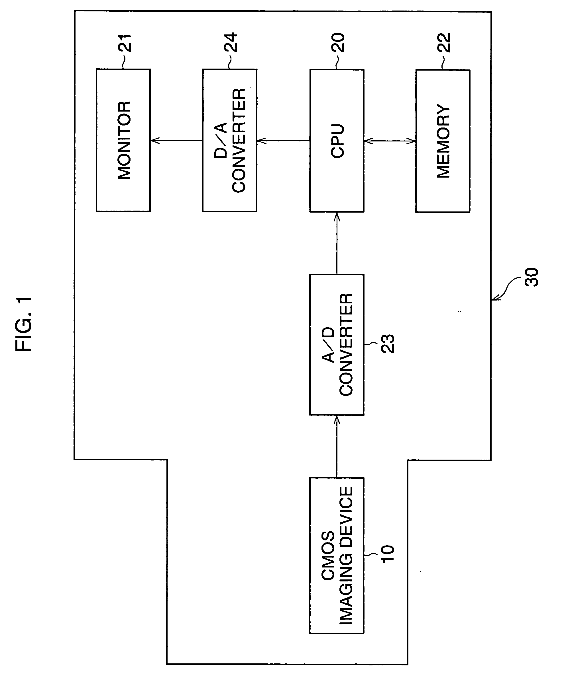
[0034]FIG. 1 schematically illustrates an electrical structure of a
[0035] The digital still camera 30 comprises a CMOS imaging device 10, a CPU 20, a monitor 21, and a memory 22. The CPU 20 is connected to the imaging device 10 via an analogue-digital (A / D) converter 23. The A / D converter 23 converts an image signal generated by the imaging device 10 from an analogue signal to a digital signal. The CPU 20 carries out some signal processes on the image signal. Some of the signal processes are, for example, a white balance process, an outline correction process, gamma correction process, Y / C separation process, and so on.
[0036] The image signal is sent to the memory 22 after the CPU 20 carries out the processes. The memory 22 stores the image signal.
[0037] Or the image signal is sent to digital-analogue (D / A) converter 24 after the CPU 20 carries out the processes. The D / A converter 24 converts the imaging signal from a digital signal to an analogue signal. The image signal from the...
third embodiment
[0083] In the third embodiment, a fourth pixel is covered with a G filter, of which the transmittance is higher than that of a second pixel. However, a fourth pixel can be covered with an R or B filter, of which the transmittance is higher than that of a first or a third pixel. In the embodiment, the fourth pixel is covered with a G filter because it is preferable for capturing an accurate image. This is because the G signal has a much wide sensitivity range for luminance signals.
[0084] In the fourth embodiment, a fourth pixel comprises a transparent and colorless material. However, a fourth pixel may not comprise any materials between the micro lens and PD. An imaging device has the same effect as the fourth embodiment as long as light transmittance in a space between a micro lens and a PD of a fourth pixel is equal for the whole range of visible light. The PD 16 in the fourth pixel can receive visible light without absorbing a particular light component, having a wavelength in the...
PUM
 Abstract
Description
Claims
Application Information