Formation of ordered thin films of organics on metal oxide surfaces

a metal oxide surface and organic semiconductor technology, applied in thermoelectric devices, solid-state devices, nano-informatics, etc., can solve the problems of low efficiency of organic semiconductor layers, large and inability to achieve very high current densities in simple holes. achieve the effect of reducing transistor curren

Inactive Publication Date: 2005-12-29
HANSON ERIC +5
View PDF22 Cites 38 Cited by
  • Summary
  • Abstract
  • Description
  • Claims
  • Application Information

AI Technical Summary

Benefits of technology

The technical effect of this patent is related to understanding the properties of transistors used in electronic circuits. Specifically, they describe a measurement called sub-threshold slope which indicates how easy it is for the transistor's current to decrease when its input signal changes from high to low. By measuring this, researchers have been able to determine the optimal way to control the behavior of the transistor and minimize power consumption. They found that the lowest possible value of sub-threshold slope depends upon certain physical factors like the material composition and structure of the transistor. Additionally, their results show that the use of a thin layer of insulation between the transistor and other components can further improve performance.

Problems solved by technology

The technical problem addressed in this patent text needs to be identified by a senior R&D personnel who has read it through.

Method used


Image

  • Formation of ordered thin films of organics on metal oxide surfaces
  • Formation of ordered thin films of organics on metal oxide surfaces
  • Formation of ordered thin films of organics on metal oxide surfaces

Examples


Embodiment Construction

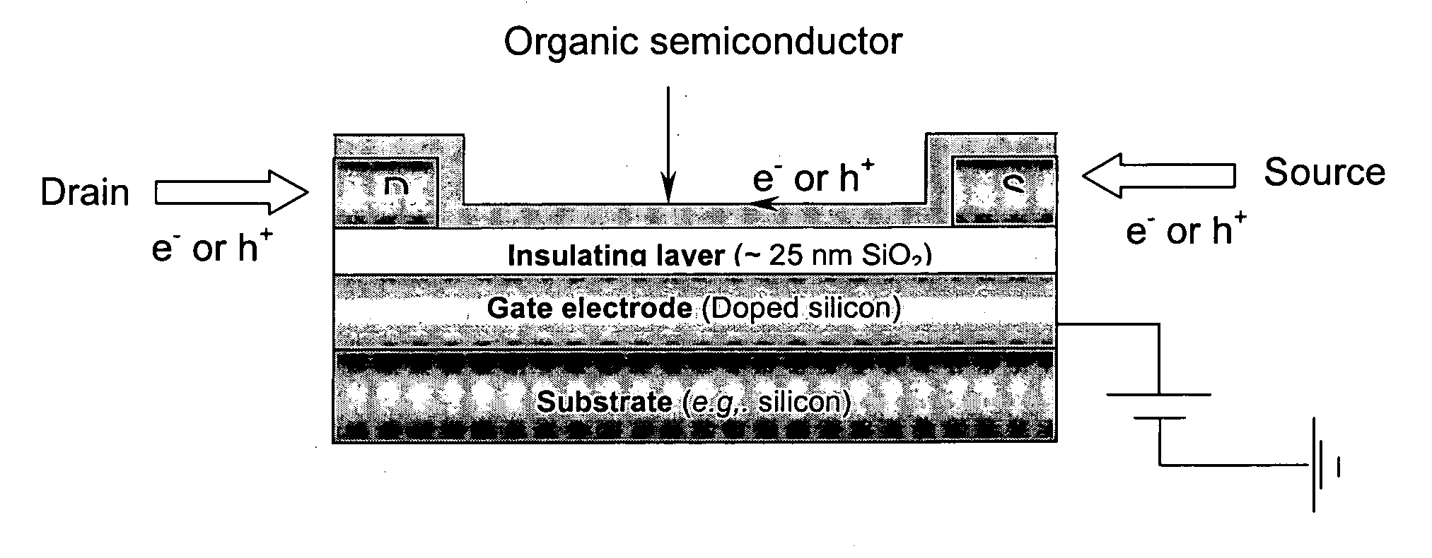
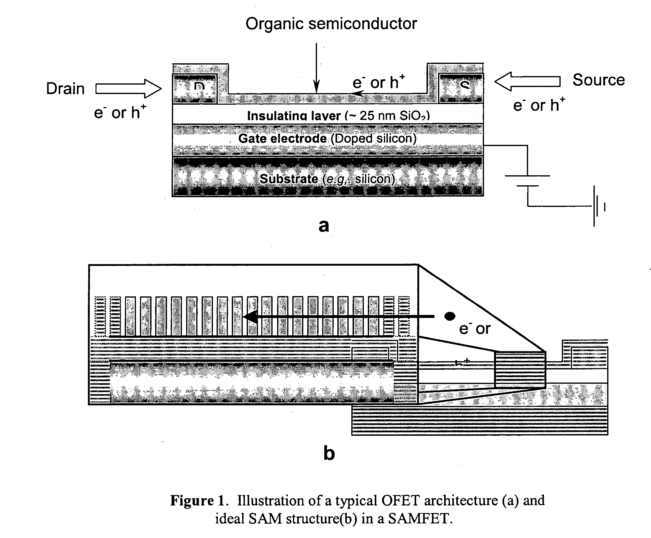
[0015] As is widely known, significant barriers to charge injection may exist at interfaces between dissimilar materials such as between inorganics and organics. Such junctions are found at the anode (for example, indium tin oxide, ITO) and cathode of organic light emitting diodes (OLEDs) or at electrodes in other novel (opto-)electronic devices comprising conjugated organic materials.1 It is therefore of interest to develop methods to suitably modify interactions at the interfaces of such dissimilar materials so that desired electronic properties of devices incorporating them can be realized. One way to accomplish this is by introducing a film, such as a self-assembled monolayer (SAM), onto the electrode surface. It is possible that charge transport across interfaces can be adjusted by the introduction of such monolayers; 2-12 these monolayers could then be further modified to enhance device function. Thus, considerable research has been reported on methods for forming films of ele...


PUM

PropertyMeasurementUnit
Fractionaaaaaaaaaa
Energyaaaaaaaaaa
Electrical conductivityaaaaaaaaaa

Abstract

Provided herein is a method for altering an electronic property of a structure comprising an oxide surface or an oxide surface in electronic communication with the structure, the method comprising providing a covalently-bound film comprising at least one organic acid residue on a portion of the oxide surface so that at least one of the following properties of the structure is modified: (a) the charge carrier injection barrier properties; (b) the charge conductivity properties; (c) the charge transport properties; (d) the work function properties; (e) the sub-threshold slope; and (f) the threshold voltage.

Description


Claims


Application Information

Patent Timeline
Owner HANSON ERIC
Why Eureka
Try Eureka