
High-frequency circuit

a high-frequency circuit and circuit technology, applied in the field of high-frequency circuits, can solve the problems of increasing process cost, limiting the length of the wire, and unable to obtain the characteristics typical of the high-frequency use of the semiconductor element, so as to prevent reflection at the connecting portion of the wire, the effect of low cost and enabling the effect of preventing reflection

Inactive Publication Date: 2005-12-29
PANASONIC CORP
View PDF4 Cites 18 Cited by
  • Summary
  • Abstract
  • Description
  • Claims
  • Application Information

AI Technical Summary

Benefits of technology

[0016] Therefore, a first object of the present invention is to provide a high-frequency circuit for enabling reflection occurring at a connecting portion of a wire to be prevented. Further, a second object of the present invention is to provide, at low cost, a high-frequency circuit for enabling the reflection occurring at the connecting portion of the wire to be prevented with high accuracy and high reliability.

Problems solved by technology

Therefore, there is a problem that characteristics typical of a semiconductor element used for high frequency cannot be sufficiently obtained.
However, there are limits to shortening the length of the wire in view of accuracy of a bonding device.
However, it is necessary to cut in a chip-mounting area on the primary mounting substrate, thereby leading to an increase in process cost.
Moreover, although a ribbon-type wire can be also used so as to reduce inductance at the connecting portion and prevent reflection, it is not preferable in view of reliable temperature change in practice.
In addition, although a flip-chip bonding using a through hole and the like can be also used so as to reduce inductance at the connecting portion and prevent reflection, it is not preferable in view of reliable temperature change in practice.

Method used


Image

  • High-frequency circuit
  • High-frequency circuit
  • High-frequency circuit

Examples


first embodiment

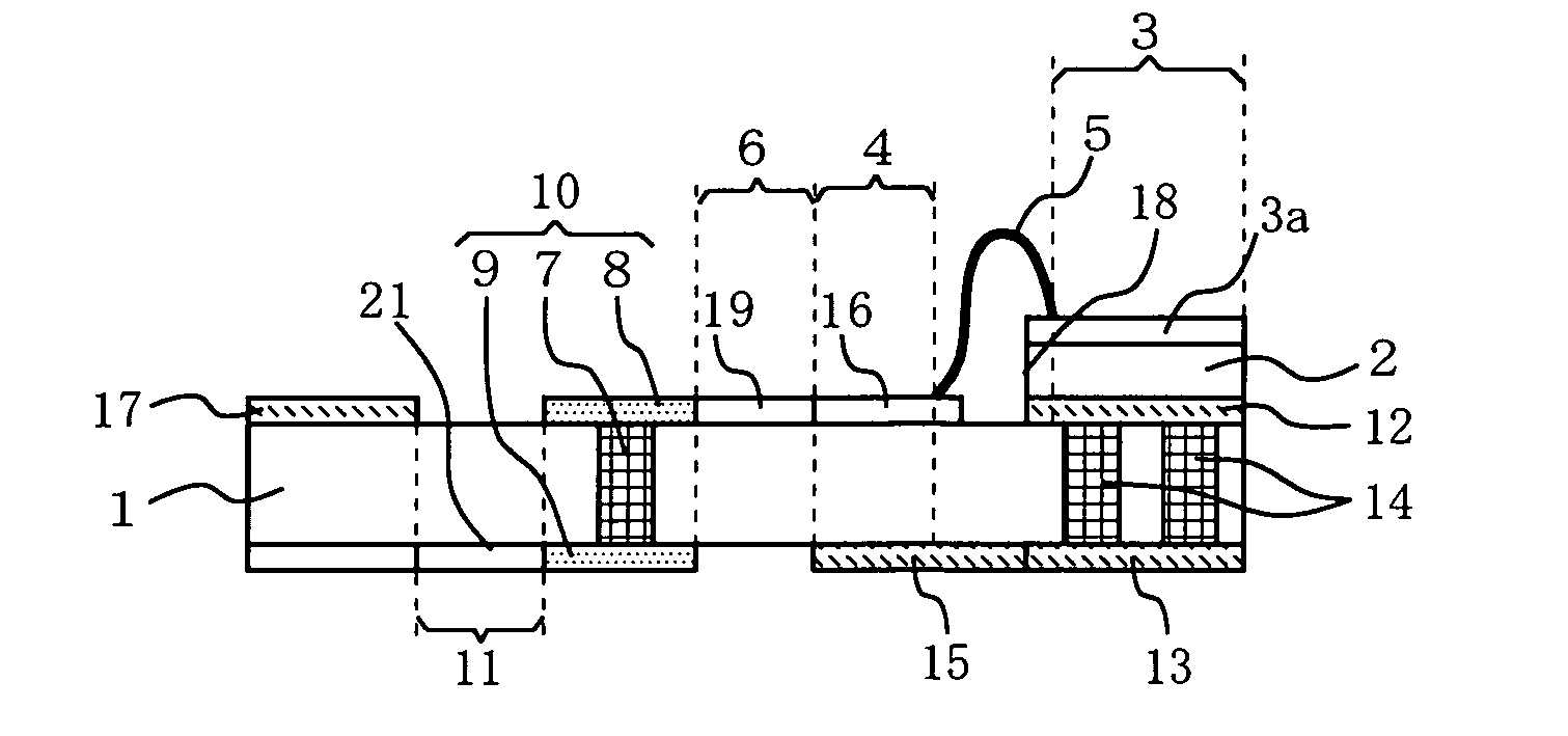
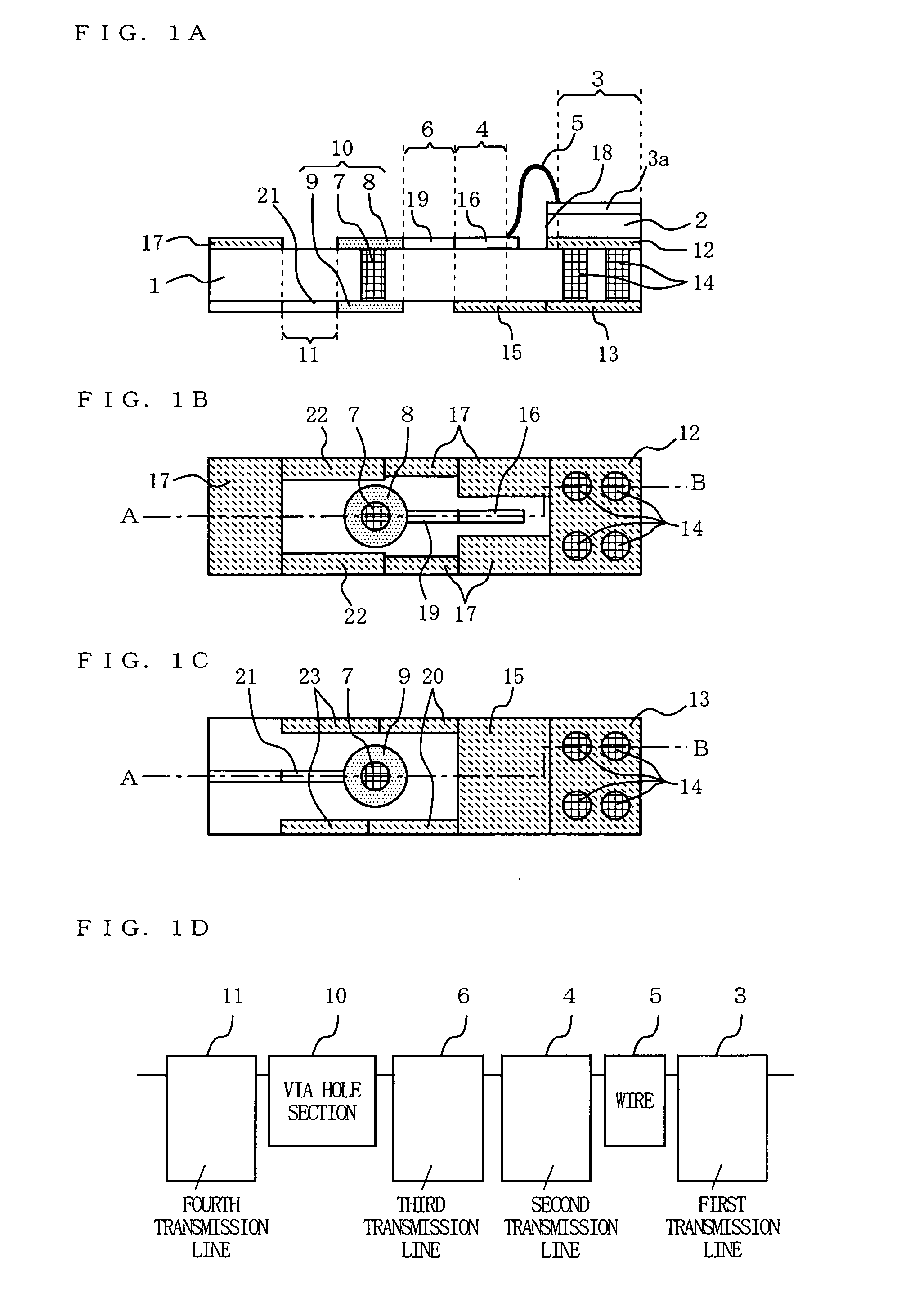
[0082]FIG. 1A is a schematic cross-sectional view illustrating an example of a high-frequency circuit according to a first embodiment of the present invention. FIG. 1B is a diagram illustrating a wiring pattern on a top surface of a dielectric substrate 1 shown in FIG. 1A. FIG. 1C is a diagram illustrating a wiring pattern on a bottom surface of the dielectric substrate 1 shown in FIG. 1A. FIG. 1D is a block diagram illustrating components of the high-frequency circuit according to the first embodiment of the present invention. FIG. 1A is also a cross-sectional view along lines AB of FIGS. 1B and C.

[0083] In FIGS. 1A to C, a high-frequency circuit according to the first embodiment comprises a dielectric substrate 1 and a high-frequency functional element 2. On a top surface of the dielectric substrate 1, ground conductive areas 12, 17, and 22, signal strips 16 and 19, and a top side conductive land 8 are formed. On a bottom surface of the dielectric substrate 1, ground conductive a...

second embodiment

[0122] Next, a high-frequency circuit according to a second embodiment of the present invention will be described. Components of the high-frequency circuit according to the second embodiment are the same as those for the first embodiment, and therefore FIG. 1A to D are also used here. The second embodiment is different from the first embodiment in that in at least a portion of the area of the fourth transmission line 11, the characteristic impedance is set so as to be higher than 50Ω in the second embodiment.

[0123]FIG. 10 is a diagram illustrating an equivalent circuit of a high-frequency circuit according to the second embodiment of the present invention. FIG. 10 shows a circuit configuration which is equivalent to a low pass filter of an LCLCL structure, the circuit configuration being obtained by adding, to the filter-type equivalent circuit of the CLCL structure according to the first embodiment shown in FIG. 9B, the fourth transmission line 11 (TRL4) which is set so as to have...

third embodiment

[0132] Next, a high-frequency circuit according to a third embodiment of the present invention will be described. Components of the high-frequency circuit according to the third embodiment are the same as those for the first embodiment, and therefore FIGS. 1A to D are also used here. The third embodiment is different from the first and second embodiments in that a characteristic impedance of the first transmission line 3 is set so as to be lower than 50Ω at a portion to which the wire is connected in the third embodiment.

[0133]FIG. 11 is a diagram illustrating an equivalent circuit of a high-frequency circuit according to the third embodiment of the present invention. FIG. 11 shows a circuit configuration which is equivalent to a low pass filter of an LCLCLC structure, the circuit configuration being obtained by adding, to the filter-type equivalent circuit of the LCLCL structure according to the second embodiment shown in FIG. 10, a wire connecting portion of the first transmissio...


PUM


Abstract

According to the present invention, provided is a high-frequency circuit having a high-frequency functional element mounted on a dielectric substrate, which comprises: a first transmission line formed in the high-frequency functional element; a second transmission line having a characteristic impedance lower than or equal to 50Ω and formed on the dielectric substrate; a wire for connecting between the first transmission line and the second transmission line; a third transmission line having a characteristic impedance higher than 50Ω and connected to the second transmission line; a via hole section which is formed so as to pass through the dielectric substrate and in which a top side conductive land is connected to the third transmission line; and a fourth transmission line connected to a bottom side conductive land of the via hole section.

Description

[0001] This application is a continuation of International Application PCT / JP2004 / 001993, filed Feb. 20, 2004.BACKGROUND OF THE INVENTION [0002] 1. Field of the Invention [0003] The present invention relates to a high-frequency circuit for use in a millimeter wave range, and more particularly to a high-frequency circuit used around portions to which a high-frequency functional element is wire-bonded. [0004] 2. Description of the Background Art [0005] In recent years, a communication speed is further increased, and thereby a carrier frequency used for radio communication is reaching a frequency band of millimeter wave domain beyond a microwave domain. As the frequency becomes higher, inductance of a wire connecting portion cannot be neglected. Therefore, reflection is increased at an input / output portion of a semiconductor element used for high frequency, the input / output portion being connected to a wire in a system. Therefore, there is a problem that characteristics typical of a se...

Claims


Application Information

Patent Timeline
Patent Type & Authority Applications(United States)
IPC IPC(8): H01L23/66H01P5/18
CPCH01L23/66H01L2223/6627H01L2224/73265H01L2224/48227H01L2224/32225H01L24/48H01P5/08H01P1/047H01L2924/3011H01L2924/30107H01L2924/19041H01L2924/19039H01L2924/19033H01L2223/6633H01L2224/48472H01L2924/01004H01L2924/01079H01L2924/09701H01L2924/14H01L2924/1423H01L2924/15311H01L2924/16152H01L2924/1903H01L2924/00H01L2224/45015H01L2224/45144H01L2924/00014H01L24/45H01L2224/45014H01L2924/20752H01L2924/206
Inventor KANNO, HIROSHI
Owner PANASONIC CORP
Learn More