Method and system for expanding flash storage device capacity

a flash storage device and capacity expansion technology, applied in the memory field, can solve the problems of increasing the density further limits the overall sd card capacity, and the limited number of chip enable signals of flash controllers, etc., to achieve the effect of increasing memory density, expanding capacity of flash storage devices, and increasing memory density

Inactive Publication Date: 2005-12-29
SUPER TALENT ELECTRONICS
View PDF4 Cites 19 Cited by
  • Summary
  • Abstract
  • Description
  • Claims
  • Application Information

AI Technical Summary

Benefits of technology

[0017] Accordingly, a system and method in accordance with the present invention provides for increased memory density within a particular space constraint by (1) providing multiple dies in a single memory package and (2) by providing stack

Problems solved by technology

Space constraints and available Flash memory density are the major obstacles in expanding the capacity of the Flash storage devices. FIG. 1 illustrates top, bottom, short side lateral and long side lateral views of a secure digital (SD) card 10.
The available Flash memory density further limits the overall SD card capacity.
In many instances, due to cost and pin count cons

Method used


Image

  • Method and system for expanding flash storage device capacity
  • Method and system for expanding flash storage device capacity
  • Method and system for expanding flash storage device capacity

Examples


Embodiment Construction

[0024] The present invention relates generally to memories and more particularly to a system and method for expanding the capacity of Flash storage devices. The following description is presented to enable one of ordinary skill in the art to make and use the invention and is provided in the context of a patent application and its requirements. Various modifications to the preferred embodiment will be readily apparent to those skilled in the art and the generic principles herein may be applied to other embodiments. Thus, the present invention is not intended to be limited to the embodiment shown but is to be accorded the widest scope consistent with the principles and features described herein.

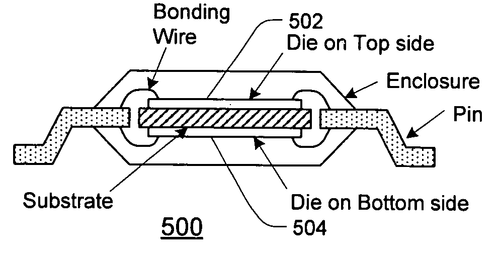
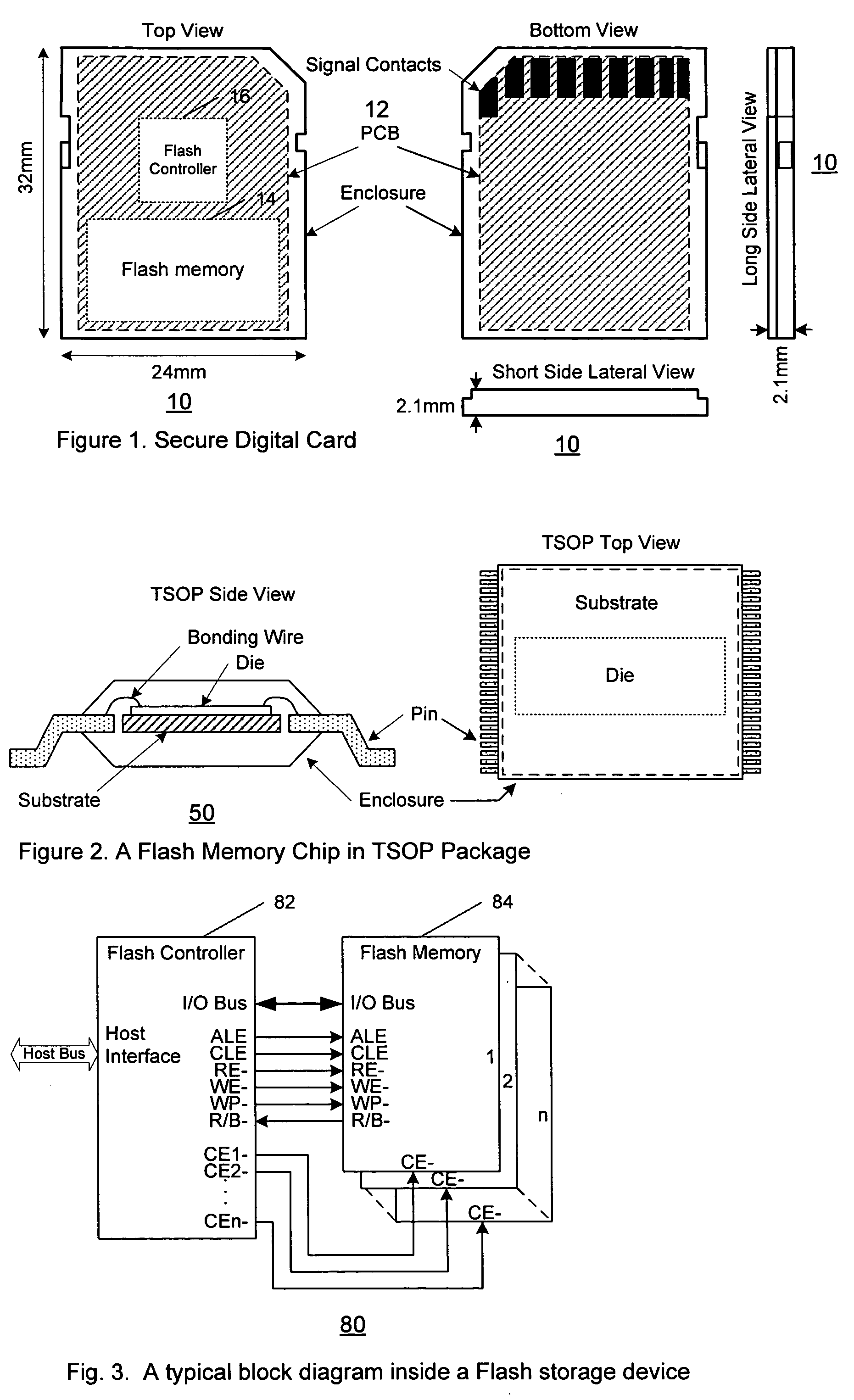
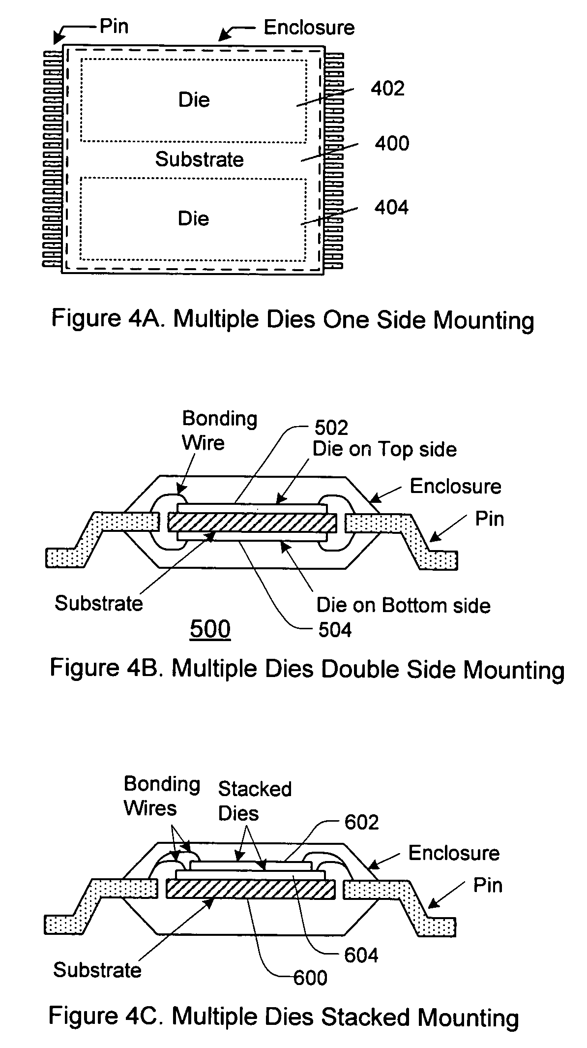
[0025] In the present invention, memory density is increased in a single package or a printed circuit board (PCB) by including more memory dies / chips on the same package / PCB. In so doing, the package / PCB will have increased memory density over a conventional package / PCB within the same space c...


PUM


Abstract

A memory package and a chip architecture which includes stacked multiple memory chips is described. In a first aspect, a memory package comprises a substrate and a plurality of memory dies mounted on the substrate. Each die has a separate chip enable. In a second aspect, a chip architecture comprises a printed circuit board (PCB). The PCB includes a footprint. The footprint includes at least one no connect (NC) pad. The chip architecture includes a plurality of stacked memory chips mounted on the printed circuit board. Each of the plurality of stacked memory has a chip enable signal pin and also has at least one NC pin. At least one of the plurality of stacked memory chips utilizes an NC pin of another of the stacked memory chips to route the chip enable pin to at least one NC pad of the footprint. Accordingly, a system and method in accordance with the present invention provides for increased memory density within a particular space constraint by (1) providing multiple dies in a single memory package and (2) by providing stacked memory chips in a single PCB footprint. In so doing, the package/PCB will have increased memory density over a conventional package/PCB within the same space constraints, and the capacity of Flash storage devices is expanded accordingly.

Description

FIELD OF THE INVENTION [0001] The present invention relates generally to memories and more particularly to a system and method for expanding the capacity of Flash storage devices. BACKGROUND OF THE INVENTION [0002] The nature of non-volatile, vibration-free, small size and low power consumption has made the Flash memory an excellent component to be utilized in various Flash storage devices. Flash storage devices are widely used as memory storage for computer and consumer system products such as notebook, desktop computer, set top box, digital camera, mobile phone, PDA and GPS etc. The increasing demand for more storage in these products has driven the need to expand the capacity of the Flash storage devices. [0003] There are two types of Flash storage devices. The first type has a pre-defined mechanical dimension. This type includes: (a) Secure Digital (SD) card, (b) Multi Media Card (MMC), (c) Memory Stick (MS) card, (d) Compact Flash (CF) card, (e) Express Flash card, (f) Serial A...

Claims


Application Information

Patent Timeline
IPC IPC(8): G11C5/04H01L23/02H01L23/495H01L23/50H01L25/10H05K1/18
CPCG11C5/04H01L2225/1058H01L23/50H01L25/105H01L2224/32145H01L2224/48091H01L2224/48247H05K1/181H05K2201/10515H05K2201/10689H01L23/49575H01L2225/1029H01L24/48H01L2924/00014H01L2924/181Y02P70/50H01L2924/00012H01L2224/45099H01L2224/45015H01L2924/207
Inventor SEE, SUN-TECKCHOU, HORNG-YEELEE, CHARLES C.
Owner SUPER TALENT ELECTRONICS
Why Eureka
Try Eureka