Non-volatile memory device with reduced distance between control gate electrode and selecting gate electrode and manufacturing method thereof

a non-volatile memory and gate electrode technology, applied in the field of memory devices, can solve problems such as the complexity of the fabrication process of memory structures, and achieve the effects of reducing the distance between the control gate electrode and the selecting gate electrode, and enhancing the density of memory cells in the non-volatile memory devi

Active Publication Date: 2019-02-05
UNITED MICROELECTRONICS CORP
View PDF4 Cites 2 Cited by
  • Summary
  • Abstract
  • Description
  • Claims
  • Application Information

AI Technical Summary

Benefits of technology

[0004]A non-volatile memory device and a manufacturing method thereof are provided by the present invention. A control gate electrode and a selecting gate electrode are separated from each other by an oxide-nitride-oxide (ONO) structure and a spacer structure in a first direction, and a distance between the control gate electrode and the selecting gate electrode in the first direction is smaller than or equal to a sum of a width of the ONO structure and a width of the spacer structure in the first direction. Accordingly, the distance between the control gate electrode and the selecting gate electrode may be reduced and the density of memory cells in the non-volatile memory device may be enhanced.

Problems solved by technology

To satisfy such trend and achieve challenge of high integration in semiconductor devices, memory miniaturization is kept on going, and thus fabrication process of memory structure is getting complicated.

Method used


Image

  • Non-volatile memory device with reduced distance between control gate electrode and selecting gate electrode and manufacturing method thereof
  • Non-volatile memory device with reduced distance between control gate electrode and selecting gate electrode and manufacturing method thereof
  • Non-volatile memory device with reduced distance between control gate electrode and selecting gate electrode and manufacturing method thereof

Examples


first embodiment

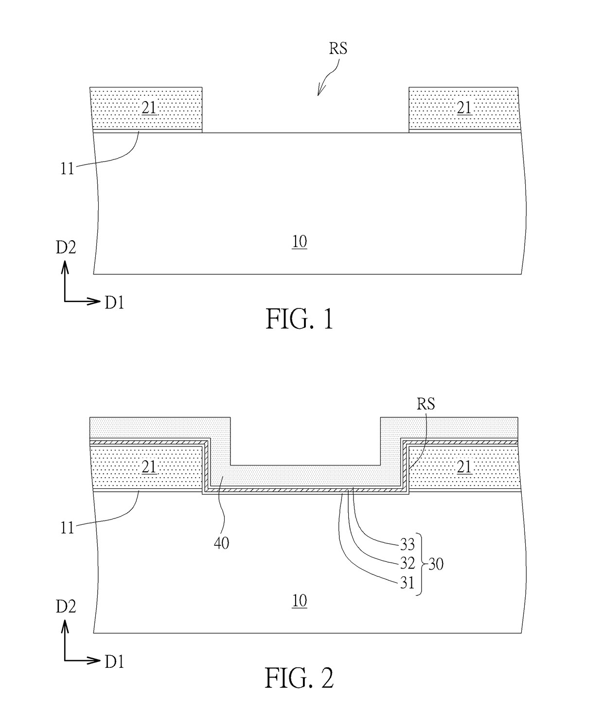
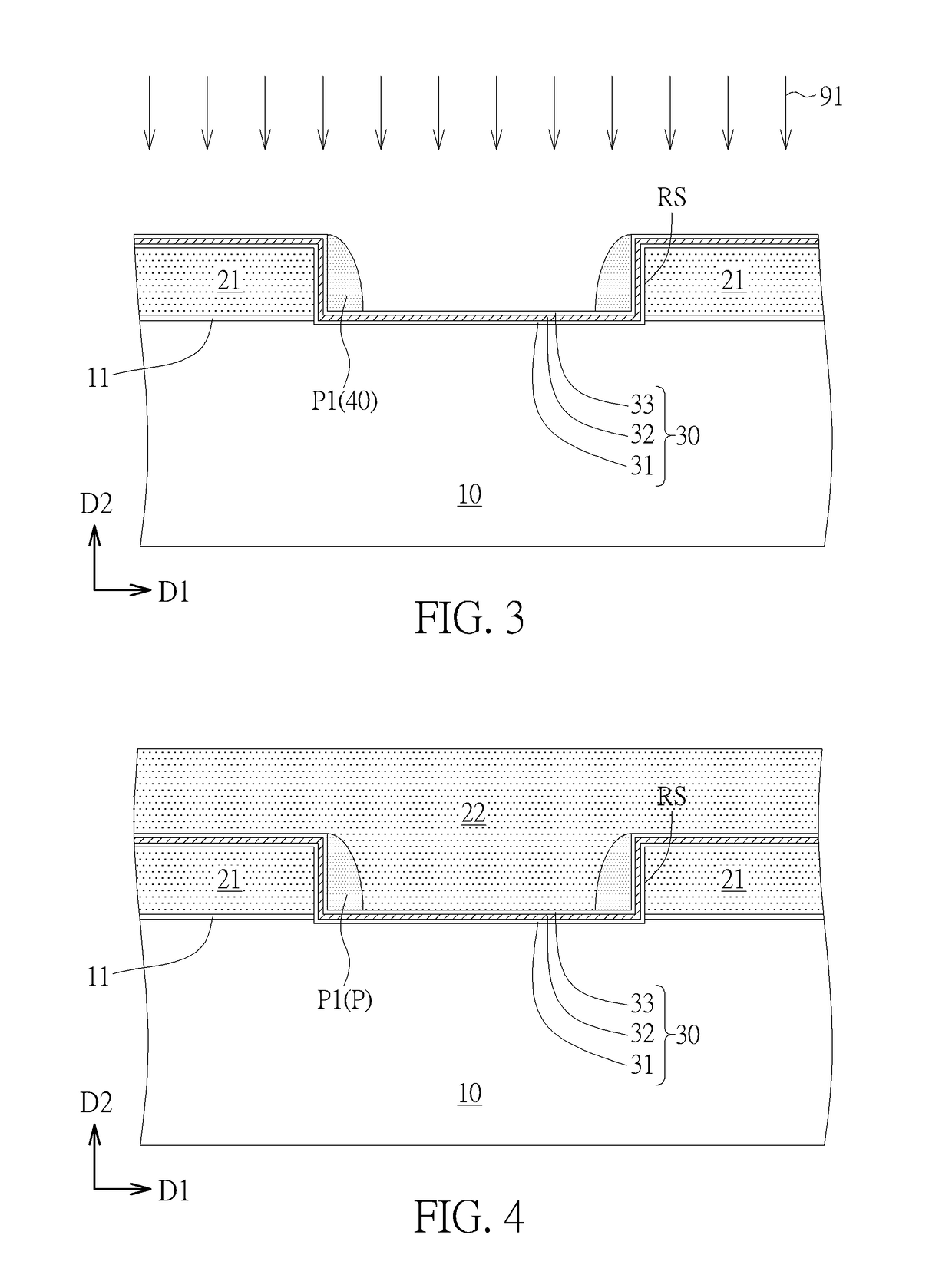
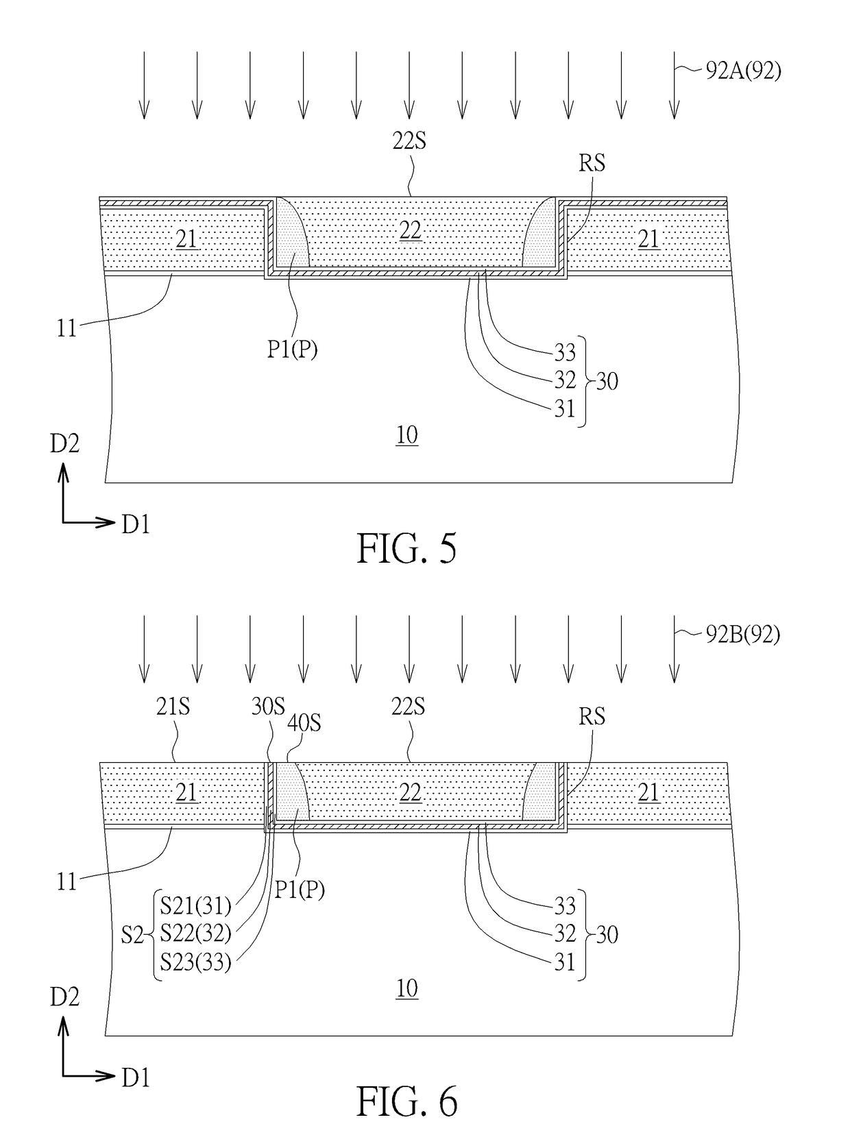
[0023]Please refer to FIGS. 1-8. FIGS. 1-8 are schematic drawings illustrating a manufacturing method of a non-volatile memory device according to the present invention. As shown in FIG. 8, the manufacturing method in this embodiment may include the following steps. A control gate electrode 22G is formed on a semiconductor substrate 10. A first oxide-nitride-oxide (ONO) structure S1 is formed between the control gate electrode 22G and the semiconductor substrate 10. A selecting gate electrode 21G is formed on the semiconductor substrate 10. A second ONO structure S2 and a spacer structure P are formed between the control gate electrode 22G and the selecting gate electrode 21G in a first direction D1. A distance DS between the control gate electrode 22G and the selecting gate electrode 21G in the first direction D1 is smaller than or equal to a sum of a width of the second ONO structure S2 (such as a first width W1 shown in FIG. 8) and a width of the spacer structure P (such as a sec...

second embodiment

[0036]Please refer to FIG. 3 and FIGS. 9-12. FIGS. 9-12 are schematic drawings illustrating a manufacturing method of a non-volatile memory device 102 according to the present invention, and FIG. 9 may be regarded as a schematic drawing in a step subsequent to FIG. 3. As shown in FIG. 3 and FIG. 9, in the manufacturing method of this embodiment, a removing process 93 may be performed to remove the second oxide layer 33 of the oxide-nitride-oxide stack layer 30 formed in the recess RS and exposed by the insulation layer 40 after the etching process 91 of forming the first spacer P1 and before the step of forming the second gate material layer (not shown in FIG. 3 and FIG. 9). In other words, a part of the second oxide layer 33 is not covered by the first spacer P1 after the etching process 91, and the second oxide layer 33 which is not covered by the first spacer P1 may be removed by the removing process 93. The removing process 93 may include an oxide pre-clean process or other appr...


PUM


Abstract

A non-volatile memory device includes a semiconductor substrate, a control gate electrode, a first oxide-nitride-oxide (ONO) structure, a selecting gate electrode, a second ONO structure, and a spacer structure. The control gate electrode and the selecting gate electrode are disposed on the semiconductor substrate. The first ONO structure is disposed between the control gate electrode and the semiconductor substrate. The second ONO structure is disposed between the control gate electrode and the selecting gate electrode in a first direction. The spacer structure is disposed between the control gate electrode and the second ONO structure in the first direction. A distance between the control gate electrode and the selecting gate electrode in the first direction is smaller than or equal to a sum of a width of the second ONO structure and a width of the spacer structure in the first direction.

Description

BACKGROUND OF THE INVENTION1. Field of the Invention[0001]The present invention relates to a memory device and a manufacturing method thereof, and more particularly, to a non-volatile memory device including an oxide-nitride-oxide (ONO) structure and a manufacturing method thereof.2. Description of the Prior Art[0002]Semiconductor memory devices are used in computer and electronics industries as a means for retaining digital information or data. Typically, the semiconductor memory devices are divided into volatile and non-volatile memory devices. The non-volatile memory devices, which can retain their data even when the power supply is interrupted, have been widely employed. As one kind of the non-volatile memory technology, a SONOS memory structure is to build a silicon nitride layer sandwiched between two silicon oxide layers for serving as the charge trapping layer while the two silicon oxide layers respectively serve as a charge tunnel layer and a charge block layer. This oxide-...

Claims


Application Information

Patent Timeline
Patent Type & Authority Patents(United States)
IPC IPC(8): H01L27/115H01L29/66H01L21/28H01L29/792H01L27/11568H01L29/423
CPCH01L27/11568H01L29/42344H01L29/66833H01L29/792H01L21/28282H01L29/40117H10B43/30
Inventor LI, KUO-LUNGSHIH, PING-CHIAHSU, WEN-PENGWANG, CHIA-WENCHEN, MENG-CHUNPAN, CHIH-HAO
Owner UNITED MICROELECTRONICS CORP
Why Eureka
Try Eureka