Resistive random access memory

a random access and memory technology, applied in the field of memory, can solve the problems of limiting the data retention capability and the storage and achieve the effect of improving the data retention capability and the memory density of the rram

Active Publication Date: 2020-08-20
WINBOND ELECTRONICS CORP
View PDF2 Cites 1 Cited by
  • Summary
  • Abstract
  • Description
  • Claims
  • Application Information

AI Technical Summary

Benefits of technology

[0003]The present invention provides an RRAM that can improve the data retention capability and the memory density of the RRAM.

Problems solved by technology

However, this configuration method limits the data retention capability and the storage density of the RRAM.

Method used


Image

  • Resistive random access memory
  • Resistive random access memory
  • Resistive random access memory

Examples


Embodiment Construction

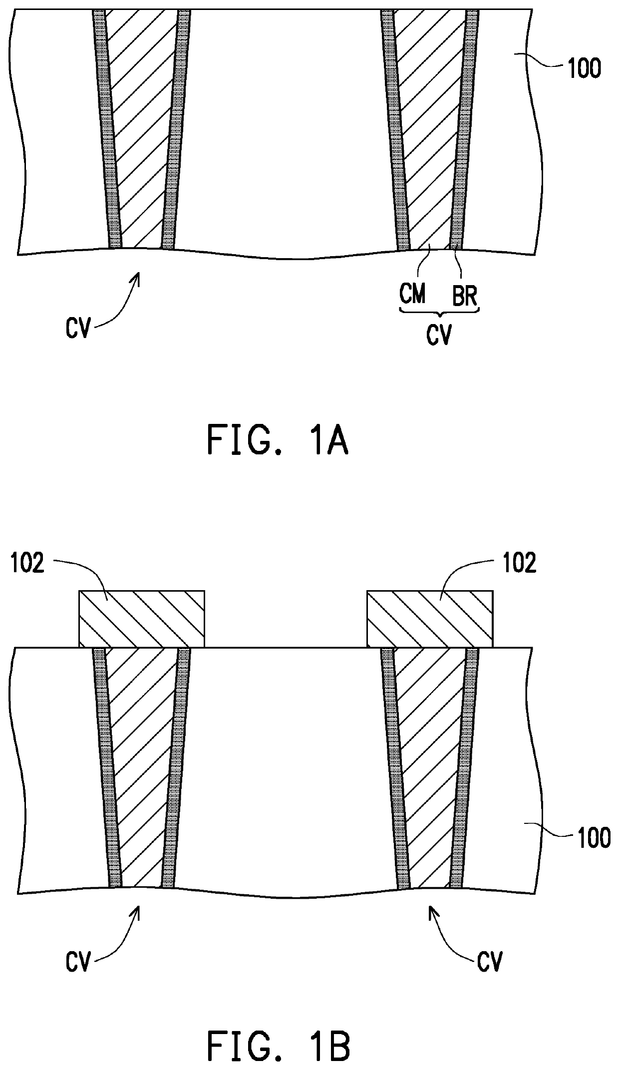
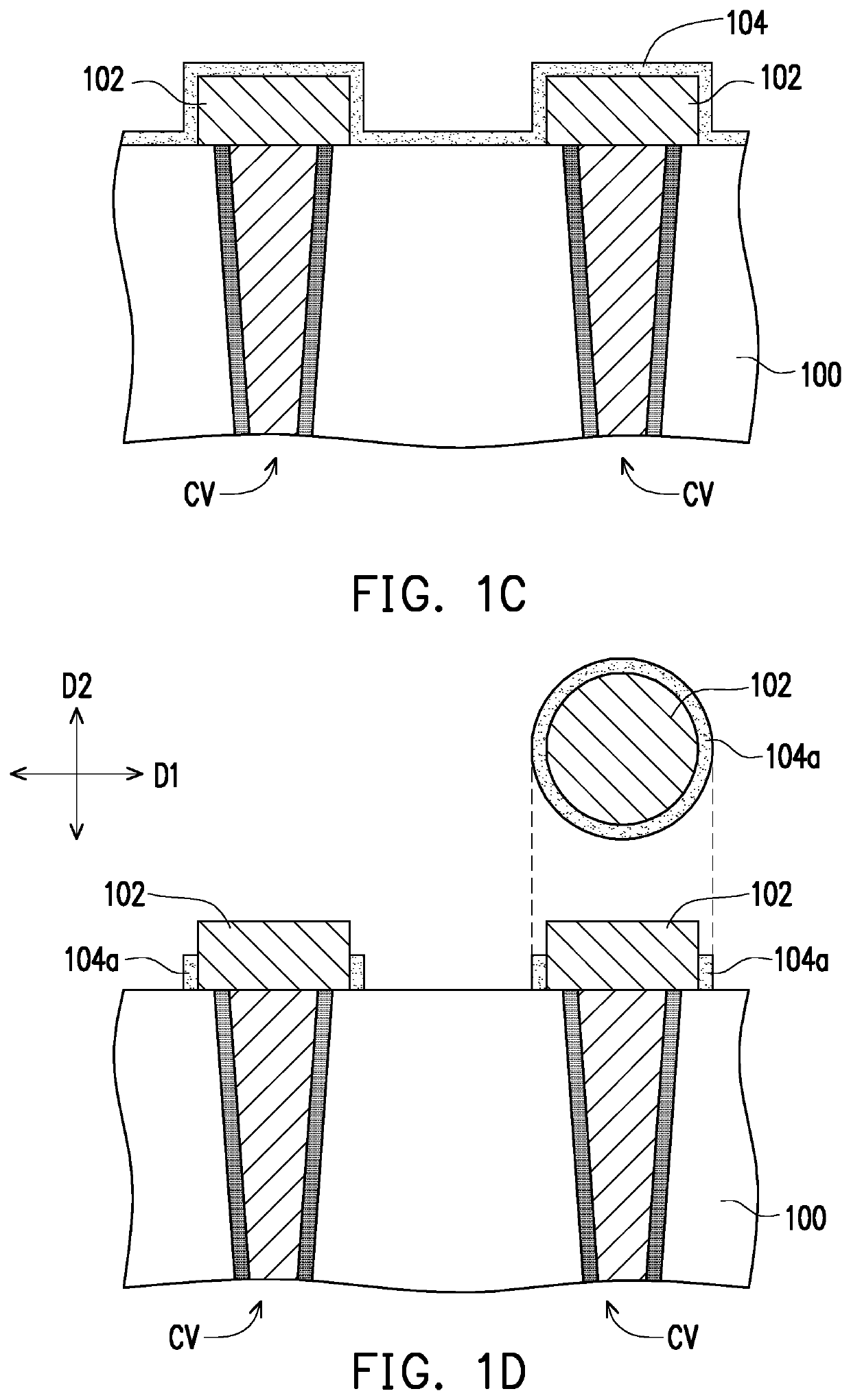
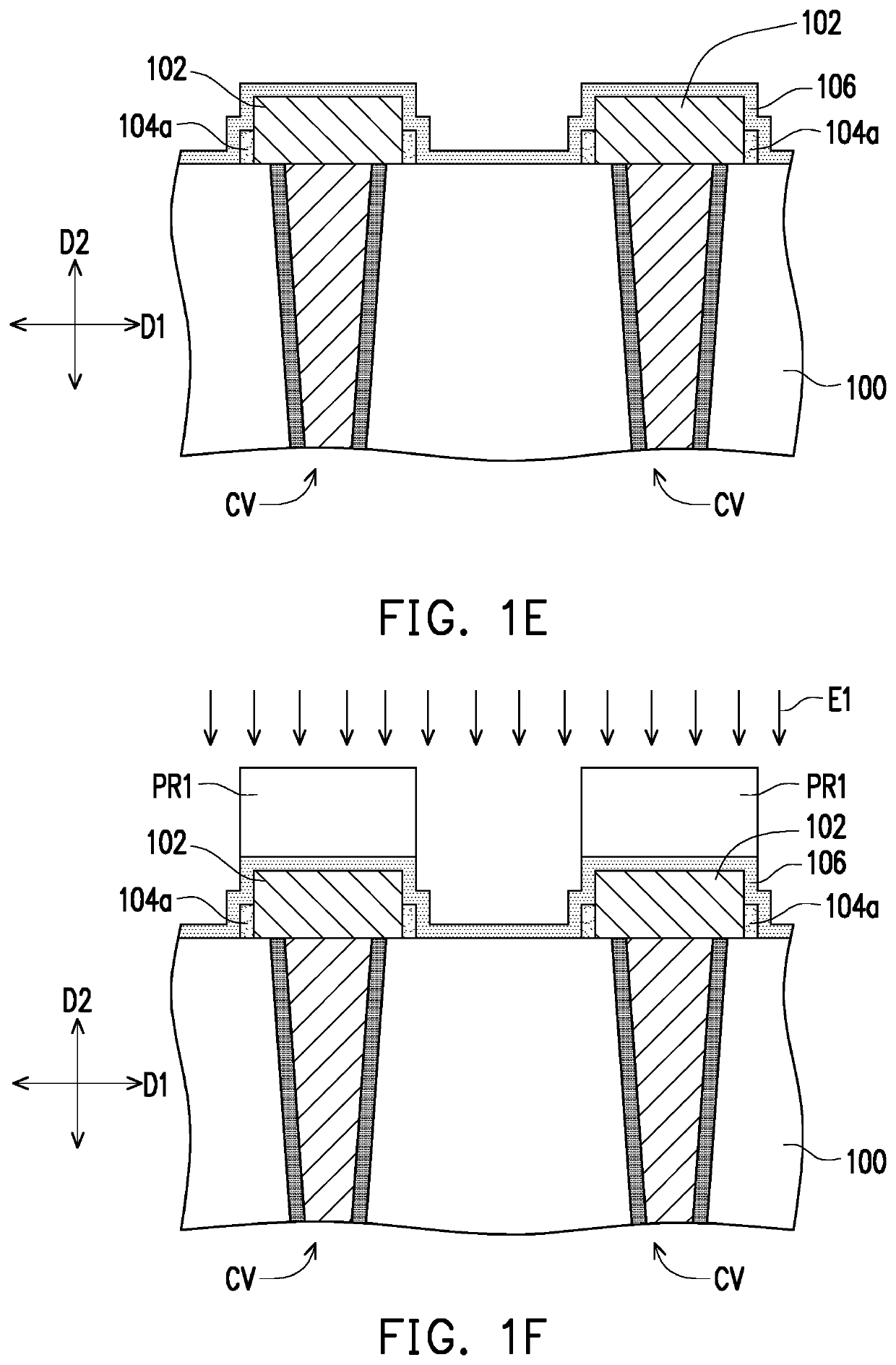
[0017]FIG. 1A to FIG. 1I are schematic cross-sectional views showing structures at various stages of a method of fabricating an RRAM 10 in accordance with some embodiments of the present invention. In some embodiments, the method of fabricating the RRAM 10 includes the following steps.

[0018]Referring to FIG. 1A, a substrate 100 is provided. In some embodiments, the substrate 100 includes a semiconductor substrate or a semiconductor on insulator (SOI) substrate. Although not shown in FIG. 1A, electronic components may have been formed in the substrate 100. In some embodiments, the electronic component comprises an active component, a passive component, or a combination thereof. For example, the active component may include a transistor, a diode, or a combination thereof. The aforementioned electronic component may be used to drive a memory component (e.g., the RRAM 10 shown in FIG. 1I) that is subsequently formed on the substrate 100. Further, an interconnect structure may be formed ...


PUM

PropertyMeasurementUnit
thicknessaaaaaaaaaa
thicknessaaaaaaaaaa
heightaaaaaaaaaa

Abstract

A resistive random access memory (RRAM) is provided. The RRAM includes a lower electrode, an upper electrode, a first variable resistance layer and a second variable resistance layer. The lower electrode is disposed on a substrate, and is a single electrode or a pair of electrodes electrically connected to each other. The upper electrode is disposed on the lower electrode, and overlaps the lower electrode. The first variable resistance layer and the second variable resistance layer are disposed on the substrate. At least a portion of the first variable resistance layer is disposed between the lower electrode and the upper electrode, and at least a portion of the second variable resistance layer is disposed between the lower electrode and the upper electrode and connected to the first variable resistance layer.

Description

BACKGROUNDTechnical Field[0001]The present invention relates to a memory and a method of fabricating the same, and more particularly to a resistive random access memory (RRAM) and a method of fabricating the same.Description of Related Art[0002]A resistive random access memory (RRAM) has the advantages of fast operation speed and low power consumption, and has become a non-volatile memory widely studied in recent years. In general, a memory cell of an RRAM circuit includes a transistor and an RRAM connected to each other. Each RRAM includes a single variable resistance layer disposed between the upper electrode and the lower electrode. However, this configuration method limits the data retention capability and the storage density of the RRAM.SUMMARY[0003]The present invention provides an RRAM that can improve the data retention capability and the memory density of the RRAM.[0004]The RRAM of the embodiment of the invention includes a lower electrode, an upper electrode, a first varia...

Claims


Application Information

Patent Timeline
Patent Type & Authority Applications(United States)
IPC IPC(8): H01L45/00G11C11/56H01L27/24
CPCH01L23/535G11C2213/52H01L45/1253G11C2213/32G11C13/0007H01L45/1608H01L45/08H01L45/1675H01L45/1233H01L45/147G11C11/5685H01L27/2463G11C2213/31H01L45/146G11C2213/50H10B63/80H10N70/24H10N70/826H10N70/043H10N70/8833H10N70/063H10N70/021H10N70/841H10N70/8836
Inventor WU, BO-LUNPAI, CHANG-TSUNGLIN, MING-CHELIN, MENG-HUNG
Owner WINBOND ELECTRONICS CORP
Why Eureka
Try Eureka