Led and fabrication method of same

a technology of led and fabrication method, which is applied in the direction of semiconductor devices, electrical devices, transistors, etc., can solve the problems of increasing the number of joint parts, increasing the thermal resistance at the time of operation, and increasing the cost of parts and assembly, so as to achieve excellent suppression of the rise in temperature resulting from heat emission, easy and compact configuration, and easy mounting on the mounting board

Inactive Publication Date: 2006-01-05
STANLEY ELECTRIC CO LTD
View PDF3 Cites 243 Cited by
  • Summary
  • Abstract
  • Description
  • Claims
  • Application Information

AI Technical Summary

Benefits of technology

[0090] In this manner, an LED and a fabrication method thereof are provided, where a rise in temperature resulting from heat emission can be excellently suppressed, where the fabrication of a multichip LED is easily possible, and which can be easily and compactly configured, and furthermore where a power of light is raised as high as possible in case of providing with a plural of LED chips, and which can be easily mounted on a mounting-board without using a bonding-wire.

Problems solved by technology

In contrast, with respect to the LED 1′, it is possible to mutually connect the LED chips 3 in series when fabricating a multichip LED because the sub-mount substrate 5 is used, but the number of parts increases, the cost of the parts and assembly costs become high, and the number of joint portions increases.
Thus, there is the problem that thermal resistance at the time of operation ends up increasing.
With respect thereto, ceramic materials such as an AlN ceramic have come to be developed as insulators with a high thermal conductivity, but there are the problems that the cost of the materials themselves is high and the processability is poor.
Moreover, with respect to the LED 1, the LED 1′ and the LED 6, there is a limit on the extent to which the chips can be made compact because it is necessary to form the horns 2a and 7a in both, and incorporating other elements and circuits inside the package has been substantially difficult.
But, in the case the partition is provided by machine-working or resin molding, the distance between each LED chip 3 is widened, so that the characteristic of the light distribution become worse and the uneven brightness occurs.
Accordingly, since a joining strength or an insulation of the above mentioned bonding wire or lead wire are insufficient, it is necessary to cover these by a resin molding or a package for protecting these bonding wire or lead wire.
So, the advantages of a small- or thin-size of the LED package cannot be utilized.
With respect of fixing the LED 1 on the mounting board 9, an adhesive is needed, and in the case that the LED is mounted adjacent to other parts such as a lens-module etc., the above mentioned bonding wire can be interfered, and it is difficult to the LED on the mounting board with maintaining the heat-radiation.

Method used


Image

  • Led and fabrication method of same
  • Led and fabrication method of same
  • Led and fabrication method of same

Examples


second embodiment

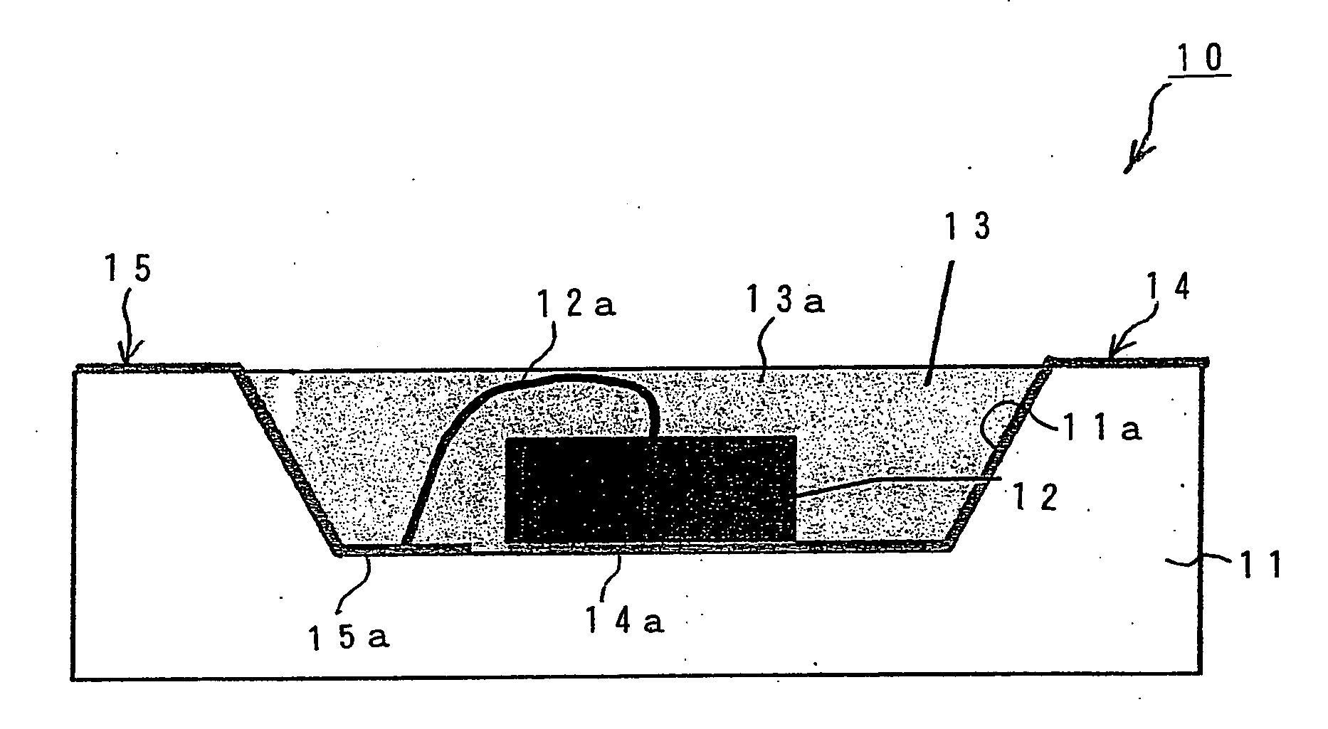
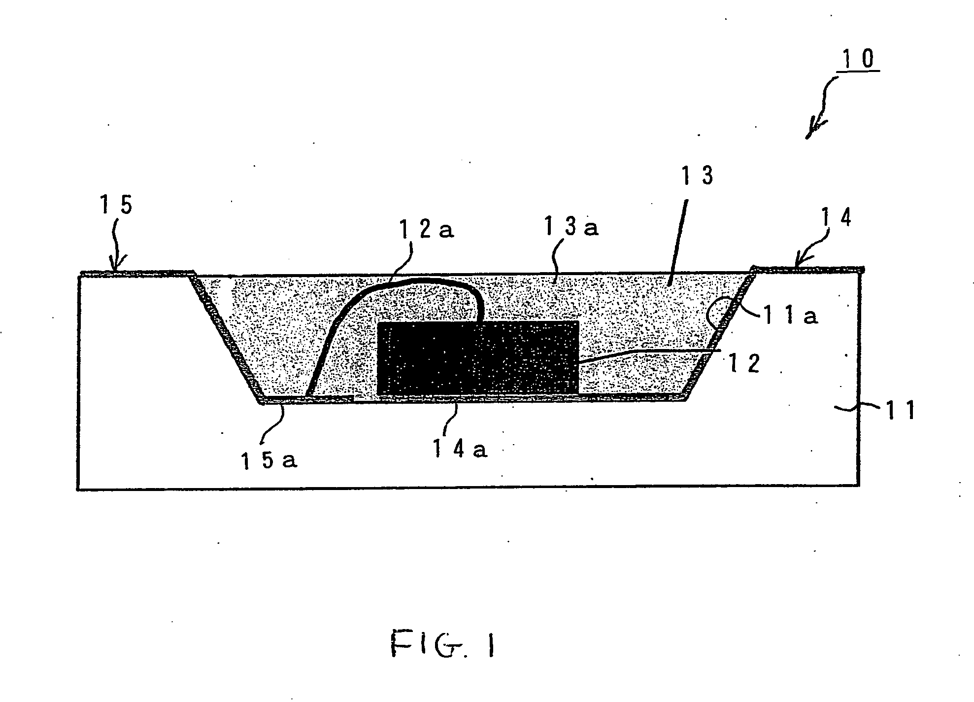
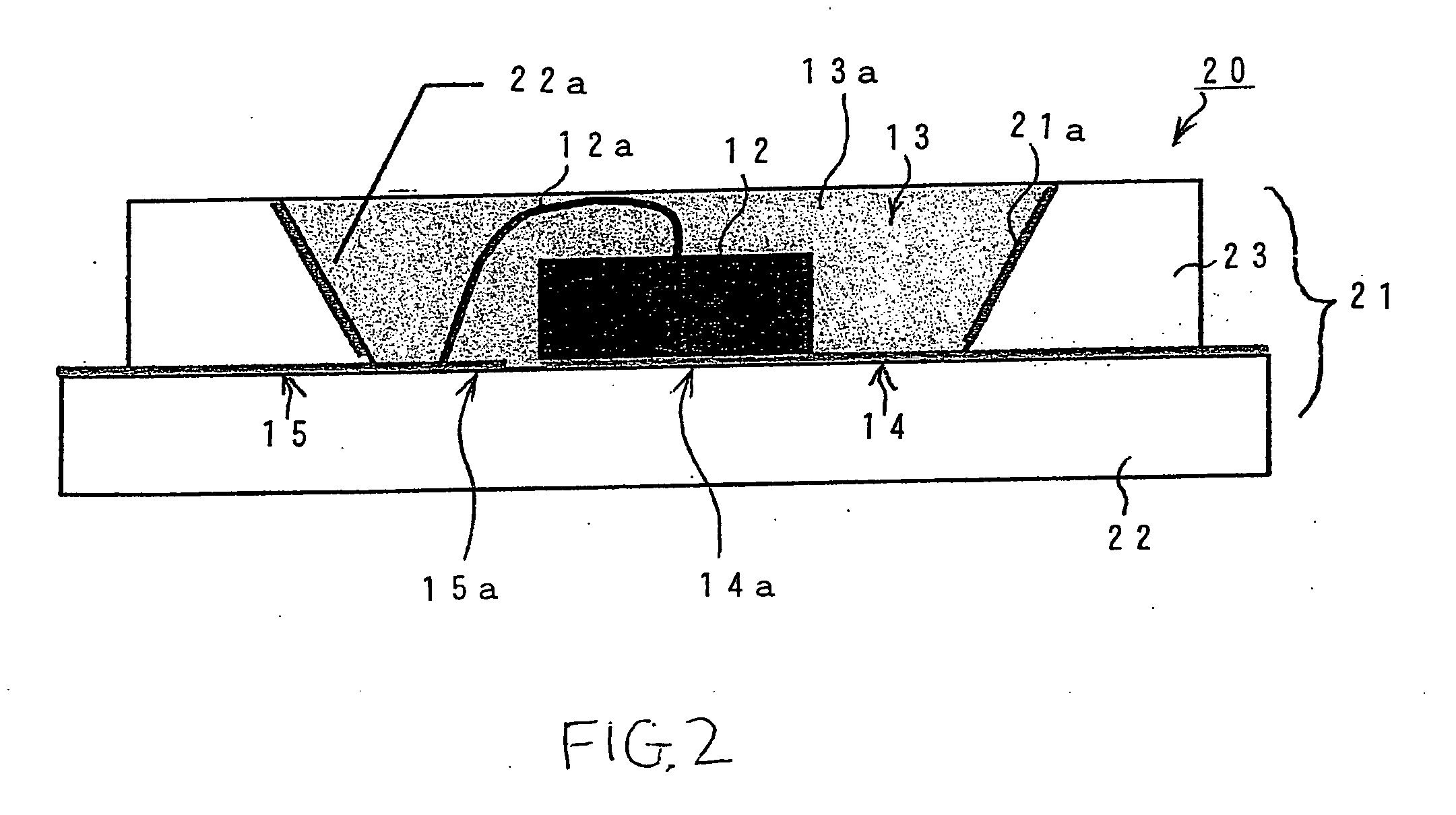
[0166]FIG. 2 shows the configuration of a second embodiment of an LED made in accordance with the principles of the invention.

[0167] As shown in FIG. 2, because an LED 20 has substantially the same configuration as that of the LED 10 shown in FIG. 1, the same reference numerals will be given to the same constituent elements and description of those same constituent elements will be omitted.

[0168] Namely, the LED 20 is configured by a silicon substrate 21, the LED chip 12 mounted inside a horn 21a formed as a concave recessed portion in the silicon substrate 21, and the resin mold 13 including a resin material filling the inside of the horn 21a.

[0169] Here, the silicon substrate 21 is configured by being laminated in two layers.

[0170] Namely, the silicon substrate 21 is configured by a lower first substrate 22 and an upper second substrate 23.

[0171] The first substrate 22 is configured by a flat silicon substrate, and the electrodes 14 and 15 are formed on the surface thereof by...

third embodiment

[0181]FIG. 3 shows the configuration of a third embodiment of an LED made in accordance with the principles of the invention.

[0182] As shown in FIG. 3, because an LED 30 has substantially the same configuration as that of the LED 20 shown in FIG. 2, the same reference numerals will be given to the same constituent elements and description of those same constituent elements will be omitted.

[0183] The LED 30 is formed so as to be disposed with chip mount portions 14b and 15b, where the electrodes 14 and 15 mutually face each other with an interval disposed therebetween, in the vicinity of the center of the upper surface of the first substrate 22.

[0184] Additionally, a so-called flip chip type LED chip 31 is mounted on and electrically connected to the tops of the chip mount portions 14b and 15b so as to ride on the electrode portions disposed at both side edges of the undersurface thereof.

[0185] According to the LED 30 of this configuration, the LED 30 acts in the same manner as t...

fourth embodiment

[0186]FIG. 4 shows the configuration of a fourth embodiment of an LED made in accordance with the principles of the invention.

[0187] As shown in FIG. 4, an LED 40 is one where a thermoelectric bimorph actuator is configured as an actuator adjacent to the horn 11a above the silicon substrate 11 with respect to the LED 10 according to FIG. 1.

[0188] The thermoelectric bimorph actuator 41 itself has a publicly known configuration and is configured by etching using the so-called MEMS technique in a semiconductor fabrication process on the silicon substrate 11.

[0189] Additionally, the thermoelectric bimorph actuator 41 is supplied with electricity via electrodes not shown, whereby, as shown in FIG. 5, it is displaced on the semiconductor substrate 11 and covers part of the upper surface of the horn 11a.

[0190] According to the LED 40 of this configuration, light is emitted to the outside from the horn 11a of the silicon substrate 11 in a manner similar to the case of the LED 10. When t...


PUM


Abstract

An LED can include a silicon substrate and a pair of electrodes formed inside a horn that is formed on the silicon substrate by anisotropic etching. The LED can include an LED chip mounted inside the horn, the LED chip being electrically connected to the pair of electrodes. A resin mold made of a resin material can be filled in the horn.

Description

[0001] This application claims the priority benefit under 35 U.S.C. §119 of Japanese Patent Application No. 2004-338624 filed on Nov. 24, 2004 and Japanese Patent Application No. 2004-046173 filed on Feb. 23, 2004, which are both hereby incorporated in their entirety by reference. BACKGROUND OF THE INVENTION [0002] 1. Field of the Invention [0003] The present invention relates to an LED and a fabrication method of the LED. [0004] 2. Description of the Related Art [0005] Conventionally, an LED such as a power white LED is configured as shown in FIG. 34. Namely, as shown in FIG. 34, an LED 1 is configured by forming a horn 2a, which results from a concave recessed portion, on a conductive substrate 2 including a metal such as copper that has a high thermal conductivity, directly mounting an LED chip 3 on the bottom surface of the horn 2a, thereafter disposing phosphors (not shown) inside the horn 2a, and covering the periphery and surface of the conductive substrate 2 with an insulato...

Claims


Application Information

Patent Timeline
Patent Type & Authority Applications(United States)
IPC IPC(8): H01L29/80H01L25/075H01L33/44H01L33/50H01L33/58H01L33/62H01L33/64
CPCH01L25/0753H01L2924/19107H01L33/58H01L33/60H01L33/642H01L2224/45144H01L2924/10253H01L2924/01322H01L2224/16225H01L2224/48091H01L2224/48227H01L2224/48465H01L33/486H01L2924/3025H01L2924/00014H01L2924/00H01L2924/181H01L2224/4903H01L2224/8592H01L2924/00012
Inventor UENO, KAZUHIKOYASUDA, YOSHIAKITANI, MASANAO
Owner STANLEY ELECTRIC CO LTD
Why Eureka
Try Eureka