Phase-change memory device and method of manufacturing the same

a memory device and phase-change technology, applied in the direction of bulk negative resistance effect devices, semiconductor devices, electrical appliances, etc., can solve the problems of consuming a reduced power, affecting the the very fast processing speed of the phase-change memory device, so as to reduce the quantity of current needed

Active Publication Date: 2006-01-12
SK HYNIX INC
View PDF2 Cites 99 Cited by
  • Summary
  • Abstract
  • Description
  • Claims
  • Application Information

AI Technical Summary

Benefits of technology

[0013] Accordingly, the present invention has been made to solve the above-mentioned problems occurring in the prior art, and an object of the present invention is to provide a phase-change memory device and method of manufacturing the same, which can reduce a contact area between a bottom electrode and a phase-change layer, thereby reducing the quantity of current necessary for phase change.

Problems solved by technology

Further, the phase-change memory device has a very fast processing speed of 5 ns, consumes a reduced power, and has a wide operation temperature range of −196˜180° C.
Further, in the ‘read’ and ‘write’ operations of the phase-change memory device, the large contact area between the bottom electrode and the phase-change layer requires an increased quantity of current for the phase change, thereby having a bad influence on the speed of the phase-change memory device.

Method used


Image

  • Phase-change memory device and method of manufacturing the same
  • Phase-change memory device and method of manufacturing the same
  • Phase-change memory device and method of manufacturing the same

Examples


Embodiment Construction

[0031] Hereinafter, a preferred embodiment of the present invention will be described with reference to the accompanying drawings. In the following description and drawings, the same reference numerals are used to designate the same or similar components, and so repetition of the description on the same or similar components will be omitted.

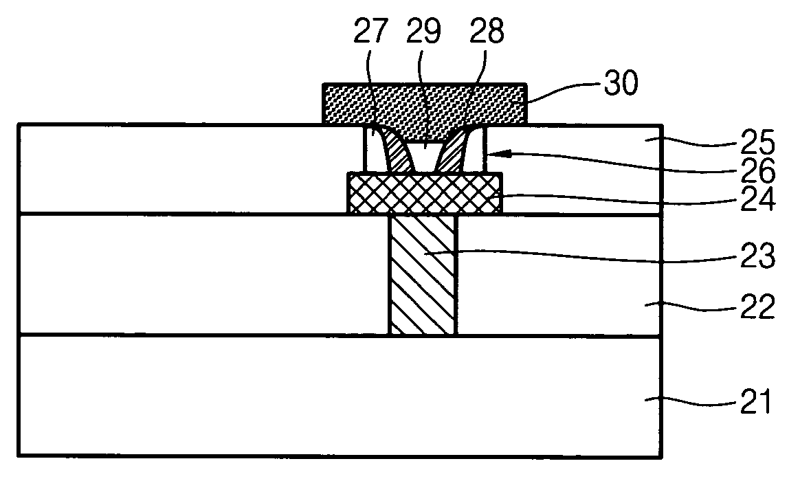
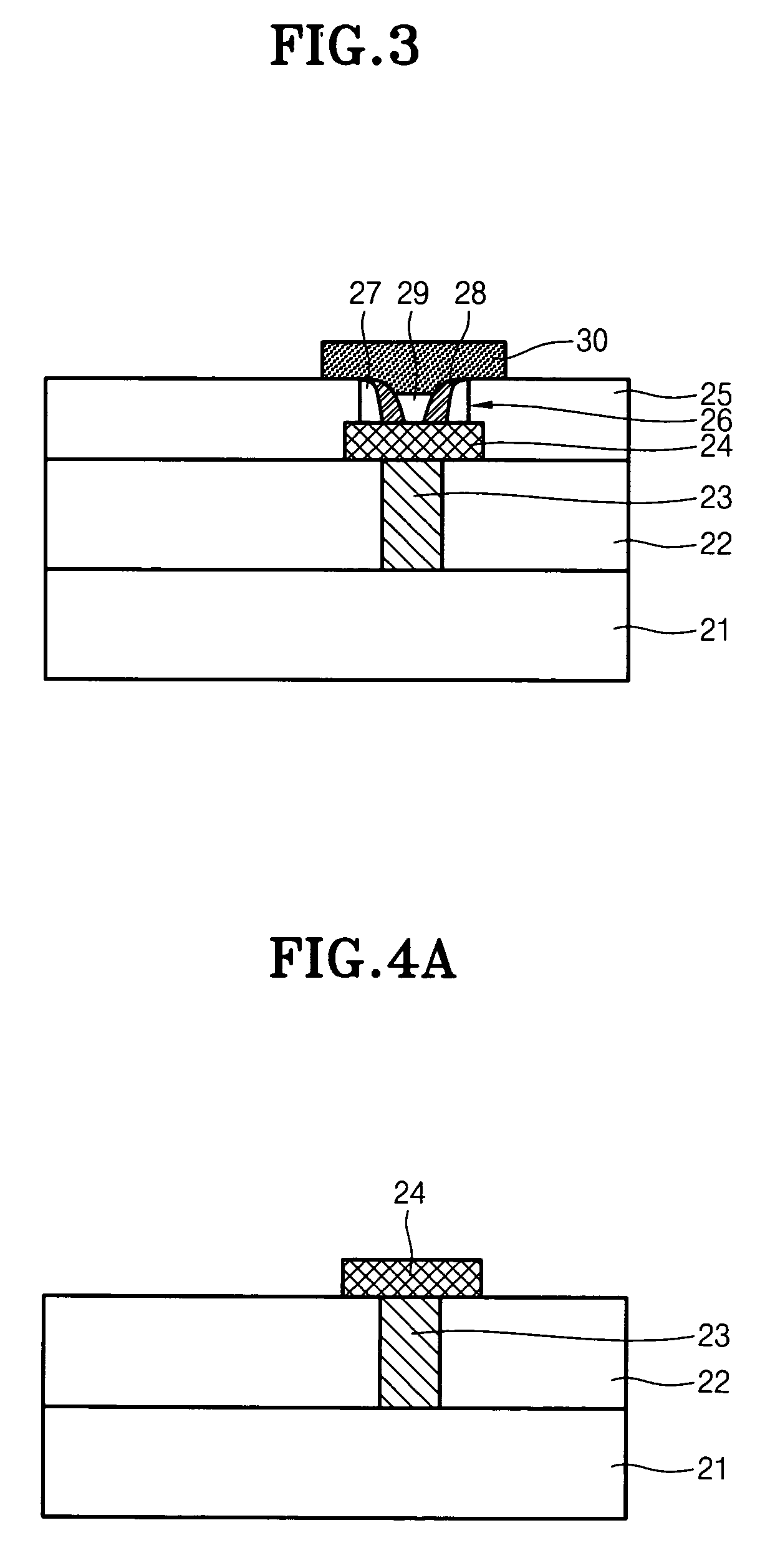
[0032]FIG. 3 is a sectional view of a phase-change memory device according to an embodiment of the present invention.

[0033] Referring to FIG. 3, in the phase-change memory device according to the present invention, a dielectric interlayer 22 is formed to cover a bottom structure (not shown) of a semiconductor substrate 21 and a contact plug 23 is then formed within the dielectric interlayer 22. Then, a bottom electrode 24 is formed on the contact plug 23 and a portion of the dielectric interlayer 22 adjacent to the contact plug 23. Then, a first oxide layer 25 is formed on the dielectric interlayer 22 and the bottom electrode 24, and a contact ...


PUM


Abstract

Disclosed are a phase-change memory device and its manufacturing method, which can reduce a contact area between a bottom electrode and a phase-change layer, thereby reducing the quantity of current necessary for phase change. The phase-change memory device comprises: a first oxide layer formed on a dielectric interlayer and a bottom electrode on a substrate and having a contact hole for exposing the bottom electrode formed in the first oxide layer; a spacer formed on a side surface of the contact hole; a phase-change layer formed on the spacer and the bottom electrode while forming a shape of another spacer; a second oxide layer filling in the contact hole while exposing an upper portion of the phase-change layer; and a top electrode formed on the first oxide layer while being in contact with the upper portion of the phase-change layer.

Description

BACKGROUND OF THE INVENTION [0001] 1. Field of the Invention [0002] The present invention relates to a phase-change memory device and method of manufacturing the same, and more particularly to a phase-change memory device and method of manufacturing the same, which can reduce a contact area between a bottom electrode and a phase-change layer, thereby reducing quantity of current. [0003] 2. Description of the Prior Art [0004] Recently, increasing attentions are paid to flash memory devices having a capability of keeping information stored therein even when power supplied thereto is interrupted. Usually, a flash memory includes a tunnel oxide layer, a floating gate, an inter-gate dielectric layer, and a control gate electrode, which are sequentially laminated on a channel. Therefore, in order to improve the reliability and program efficiency of the flash memory devices, it is necessary to improve the film quality of the tunnel oxide layer and increase a coupling rate of each cell. [00...

Claims


Application Information

Patent Timeline
Patent Type & Authority Applications(United States)
IPC IPC(8): H01L29/02
CPCH01L45/06H01L45/1691H01L45/124H10N70/8265H10N70/828H10N70/231H10N70/068
Inventor CHANG, HEON YONG
Owner SK HYNIX INC
Why Eureka
Try Eureka