

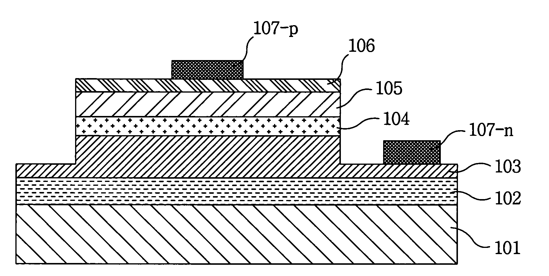
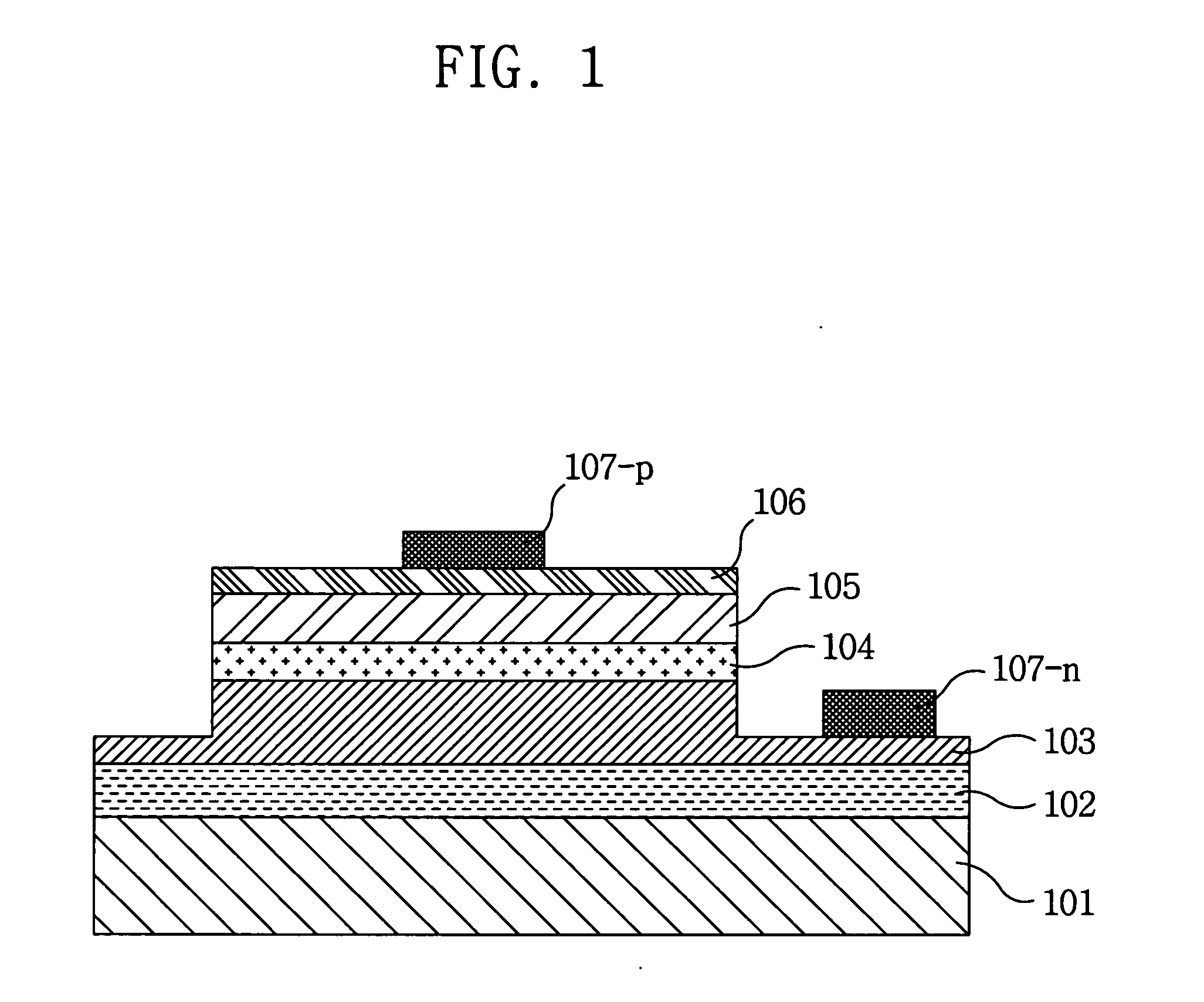
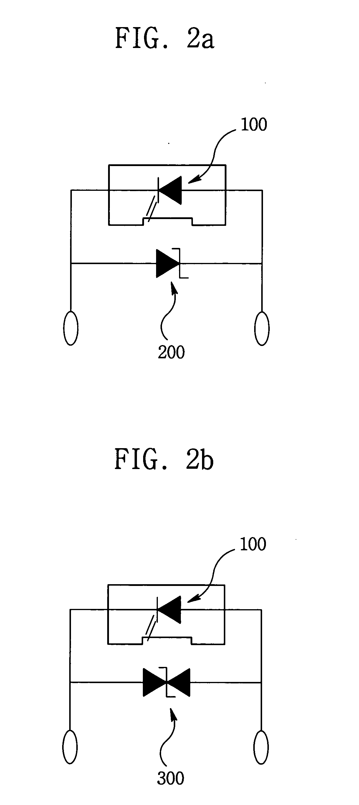
Submount substrate for mounting light emitting device and method of fabricating the same
a technology substrates, which is applied in the direction of semiconductor devices, electrical devices, transistors, etc., can solve the problems of failure of light emitting devices, inability to reduce manufacturing costs, and worse problems, so as to reduce the process of diffusion masks and reduce manufacturing costs
- Summary
- Abstract
- Description
- Claims
- Application Information
AI Technical Summary
Benefits of technology
Problems solved by technology
Method used
Image

Examples
first embodiment
[0042]FIGS. 4a to 4g are cross-sectional views illustrating a method of fabricating a submount substrate for mounting a light emitting device according to the present invention, and show a process of fabricating the submount substrate for mounting the light emitting device in which a Zener diode capable of protecting a light emitting device from a surge voltage or static electricity is integrated, using a silicon bulk micromachining process.
[0043] Referring to FIG. 4a, a substrate (300) doped with first polar impurities is first prepared.
[0044] Preferably, the substrate (300) is a silicon substrate.
[0045] Then, on the top and bottom surfaces of the substrate (300) are injected and diffused second impurities having the polarity different from that of the first polar impurities to form first and second diffusion layers (310. 311). (see FIG. 4b)
[0046] At this time, the second polar impurities can be injected and diffused into the top and bottom surfaces of the substrate (310) withou...
second embodiment
[0066]FIGS. 7a to 7i are cross-sectional views illustrating a method of fabricating a submount substrate for mounting a light emitting device in which a Zener diode having a bi-directional threshold voltage characteristic is integrated according to the present invention. Herein, a PNP (or NPN) Zener diode is used as the Zener diode having the bi-directional threshold voltage characteristic.
[0067] First, a substrate (300) doped with first polar impurities is prepared. (see FIG. 7a)
[0068] Preferably, the substrate (300) is a silicon substrate.
[0069] Then, on the top and bottom surfaces of the substrate (300) are injected and diffused second impurities having the polarity different from that of the first polar impurities to form first and second diffusion layers (310. 320). (see FIG. 7b)
[0070] Successively, mask layers (510. 520) are formed on the top and bottom surfaces of the substrate (300), respectively. Some parts of the mask layer (510) formed on the top surface of the substra...
PUM
 Abstract
Description
Claims
Application Information