Physical quantity sensor and method for manufacturing the same

Inactive Publication Date: 2006-01-12
DENSO CORP
View PDF6 Cites 4 Cited by
  • Summary
  • Abstract
  • Description
  • Claims
  • Application Information

AI Technical Summary

Benefits of technology

[0007] In the above sensor, the height of the movable portion is constant so that the shape of the movable portion is accurately formed. Thus, the sensor has the homogeneous movable portion.
[0009] In the above sensor, the height of the movable portion is constant so that the shape of the movable portion is accurately formed. Thus, the sensor has the homogeneous movable portion.
[0011] The above method provides the sensor having a constant height of the movable portion so that the shape of the movable portion is accurately formed. Thus, the sensor has the homogeneous movable portion.
[0013] The above method provides the sensor having a constant height of the movable portion so that the shape of the movable portion is accurately formed. Thus, the sensor has the homogeneous movable portion.

Problems solved by technology

However, it is difficult to control the clearance L accurately.
Thus, it is difficult to control the capacitance and the like accurately, so that the device design is restricted.

Method used


Image

  • Physical quantity sensor and method for manufacturing the same
  • Physical quantity sensor and method for manufacturing the same
  • Physical quantity sensor and method for manufacturing the same

Examples


first embodiment

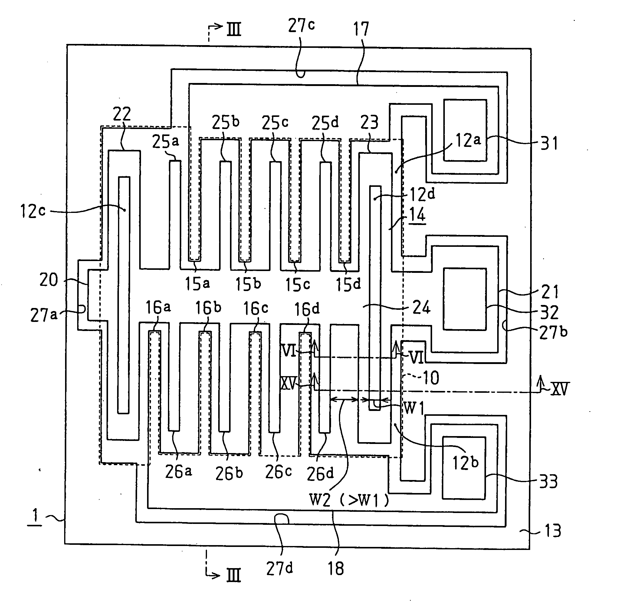
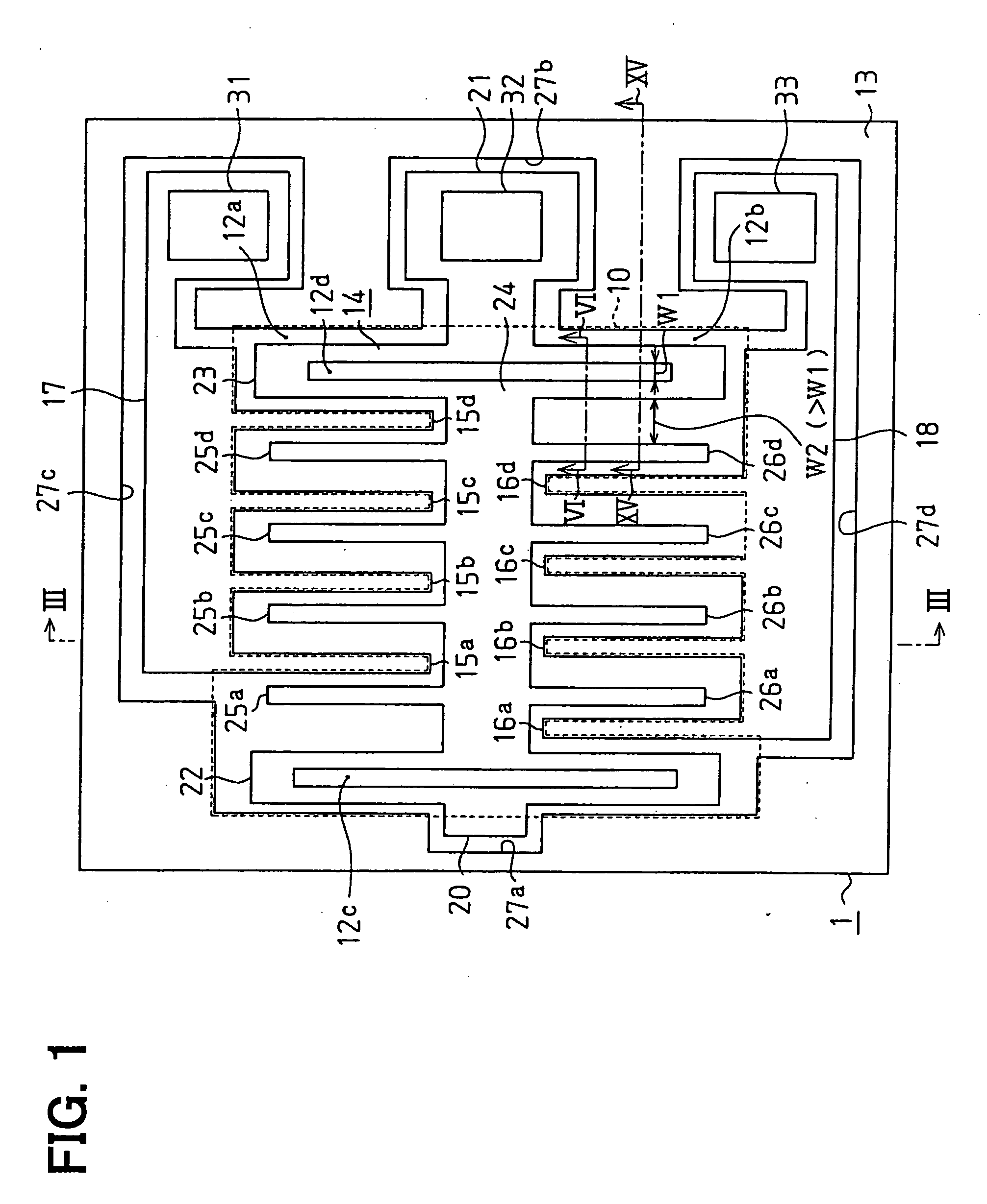
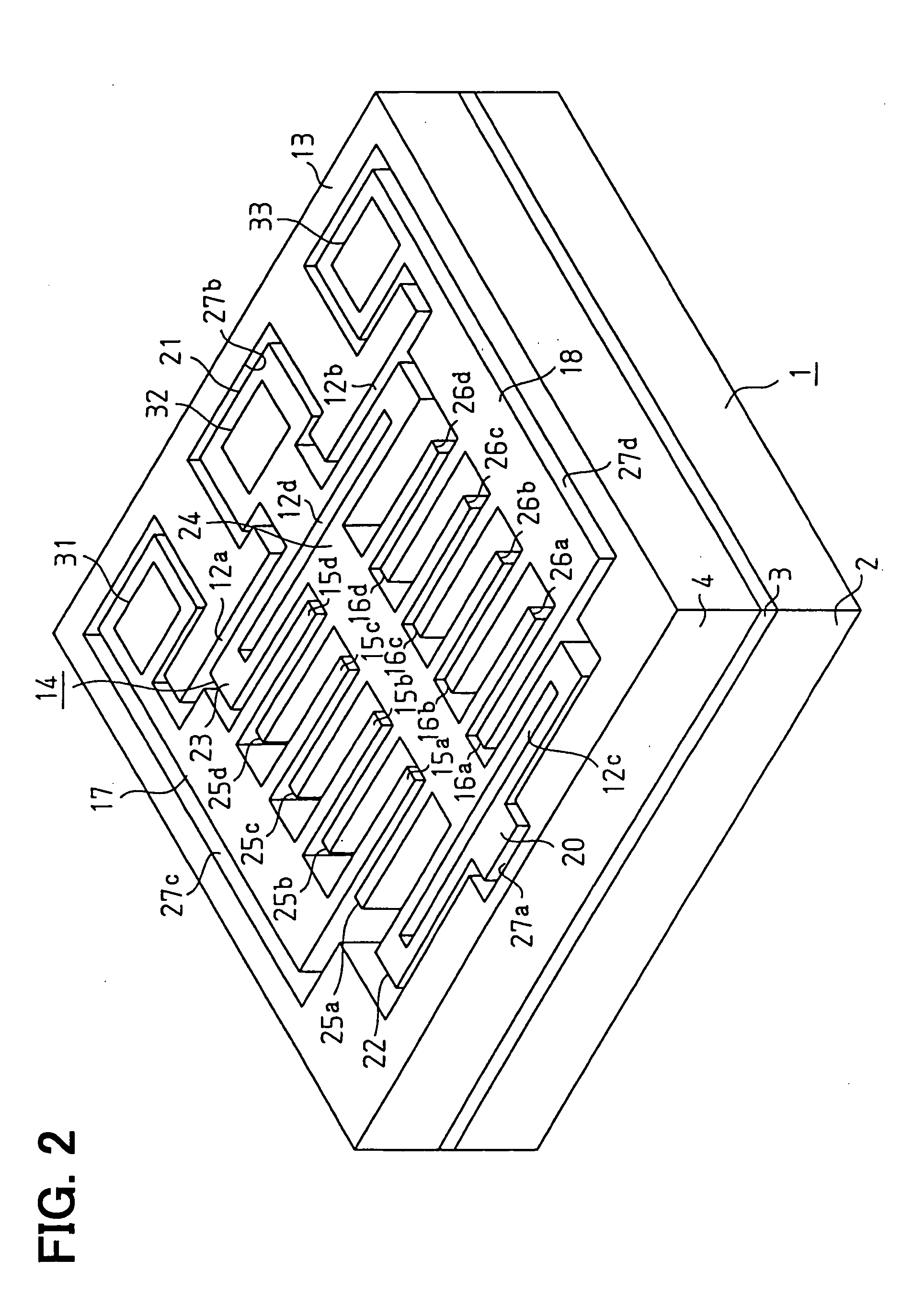
[0036] A semiconductor acceleration sensor according to a preferred embodiment of the present invention is shown in FIGS. 1 to 3. As shown in FIG. 3, the sensor includes a multi-layered substrate 1, which is made of SOI substrate. The multi-layered substrate 1 includes a silicon substrate 2, an embedded oxide film 3, and a silicon layer 4, which are stacked in this order. Specifically, the silicon layer 4 is disposed on the silicon substrate 2 through the embedded oxide film 3. The embedded oxide film 3 is made of SiO2 film. A cavity 10 is formed between the silicon layer 4 and the embedded oxide film 3. The cavity 10 has a predetermined thickness T0. Further, the cavity 10 extends in a horizontal direction, i.e., a lateral direction of the multi-layered substrate 1. In FIG. 1, a cavity formation region is shown as a broken line.

[0037] Grooves 12a-12d are formed in the silicon layer 4 of the multi-layered substrate 1. Specifically, the grooves 12a-12d are formed over the cavity 10....


PUM


Abstract

A physical quantity sensor includes: a semiconductor substrate; a cavity disposed in the substrate and extending in a horizontal direction of the substrate; a groove disposed on the substrate and reaching the cavity; a movable portion separated by the cavity and the groove so that the movable portion is movably supported on the substrate; and an insulation layer disposed on a bottom of the movable portion so that the insulation layer provides a roof of the cavity.

Description

CROSS REFERENCE TO RELATED APPLICATIONS [0001] This application is based on Japanese Patent Applications No. 2004-199738 filed on Jul. 6, 2004, and No. 2005-160599 filed on May 31, 2005, the disclosures of which are incorporated herein by references. FIELD OF THE INVENTION [0002] The present invention relates to a physical quantity sensor. Further, the present invention relates to a method for manufacturing a physical quantity sensor. BACKGROUND OF THE INVENTION [0003] A semiconductor physical quantity sensor having a beam structure in a semiconductor substrate is manufactured by using a micro machining method. This type of sensor is disclosed in, for example, U.S. Pat. No. 6,399,516. When the sensor is manufactured, as shown in FIG. 20A, a SOI substrate is used. The SOI substrate includes a silicon substrate 200, an embedded oxide film 201 and a silicon layer 202, which are stacked in this order. The silicon layer 202 in the SOI substrate is etched so that a groove 210 as a trench ...

Claims


Application Information

Patent Timeline
IPC IPC(8): H01L21/306G01P15/125
CPCB81B2201/0235B81B2201/0292B81B2203/0118B81C1/00626G01P2015/0814B81C2201/019G01P15/0802G01P15/125B81C2201/014
Inventor ASAI, MAKOTO
Owner DENSO CORP
Why Eureka
Try Eureka