Method for forming robust solder interconnect structures by reducing effects of seed layer underetching

a solder interconnect and seed layer technology, applied in the field of semiconductor device processing, can solve the problems of incomplete blm in terms, defects in the integrity of c4 joint reliability, and undercutting of the cu and crcu portions of the seed layer with respect to the ni/cu barrier layer,

Inactive Publication Date: 2006-01-12
INVENSAS CORP
View PDF8 Cites 6 Cited by
  • Summary
  • Abstract
  • Description
  • Claims
  • Application Information

AI Technical Summary

Problems solved by technology

Unfortunately, during the electroetching process, there is an undercut of the Cu and CrCu portions of the seed layer with respect to the Ni / Cu barrier layer.
This results in an incomplete BLM in terms of the layers (TiW / CrCu / Cu / Ni) defined under the solder bump.
These defects are problematic in terms of the integrity of C4 joint reliability.

Method used


Image

  • Method for forming robust solder interconnect structures by reducing effects of seed layer underetching
  • Method for forming robust solder interconnect structures by reducing effects of seed layer underetching
  • Method for forming robust solder interconnect structures by reducing effects of seed layer underetching

Examples


Embodiment Construction

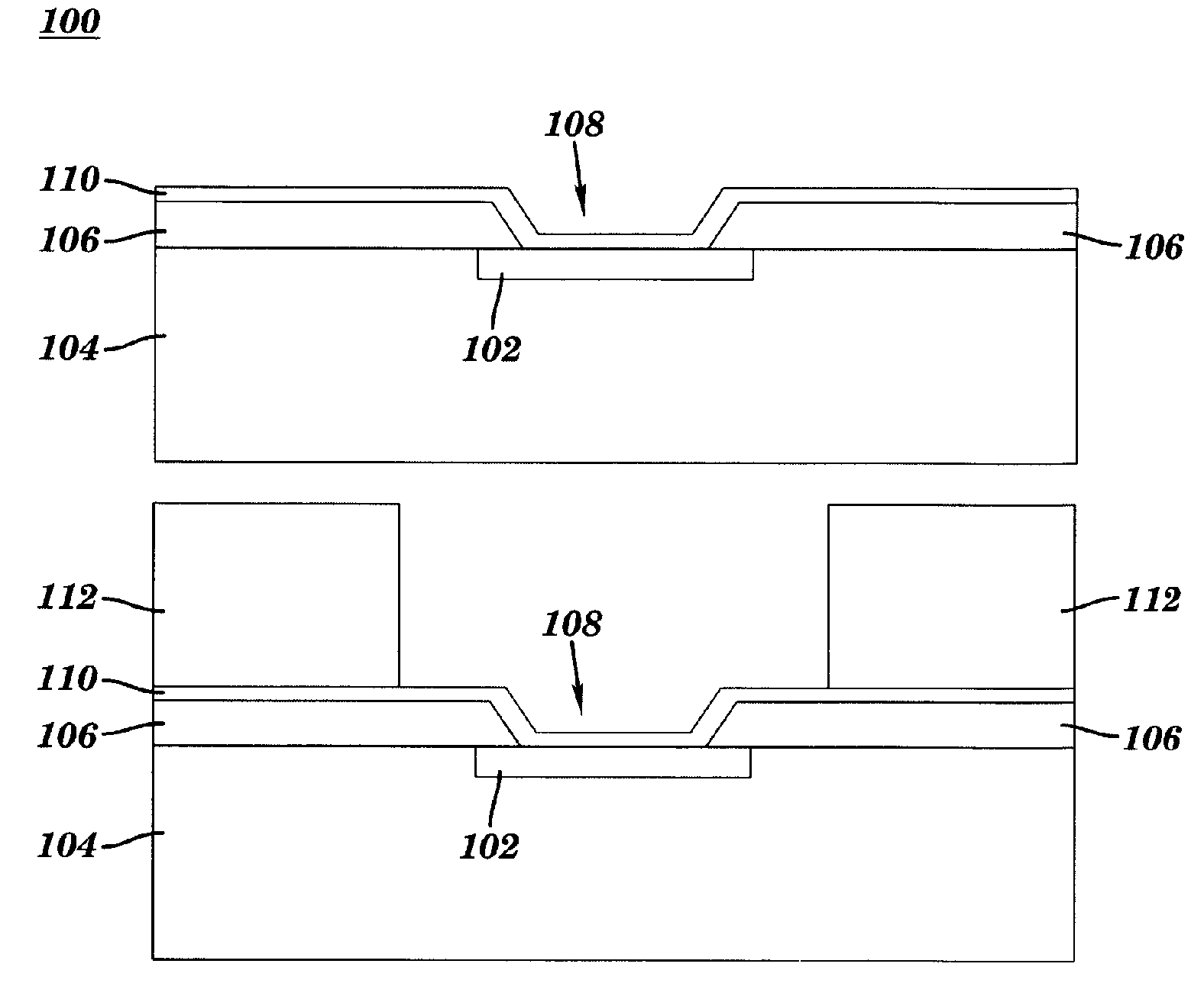
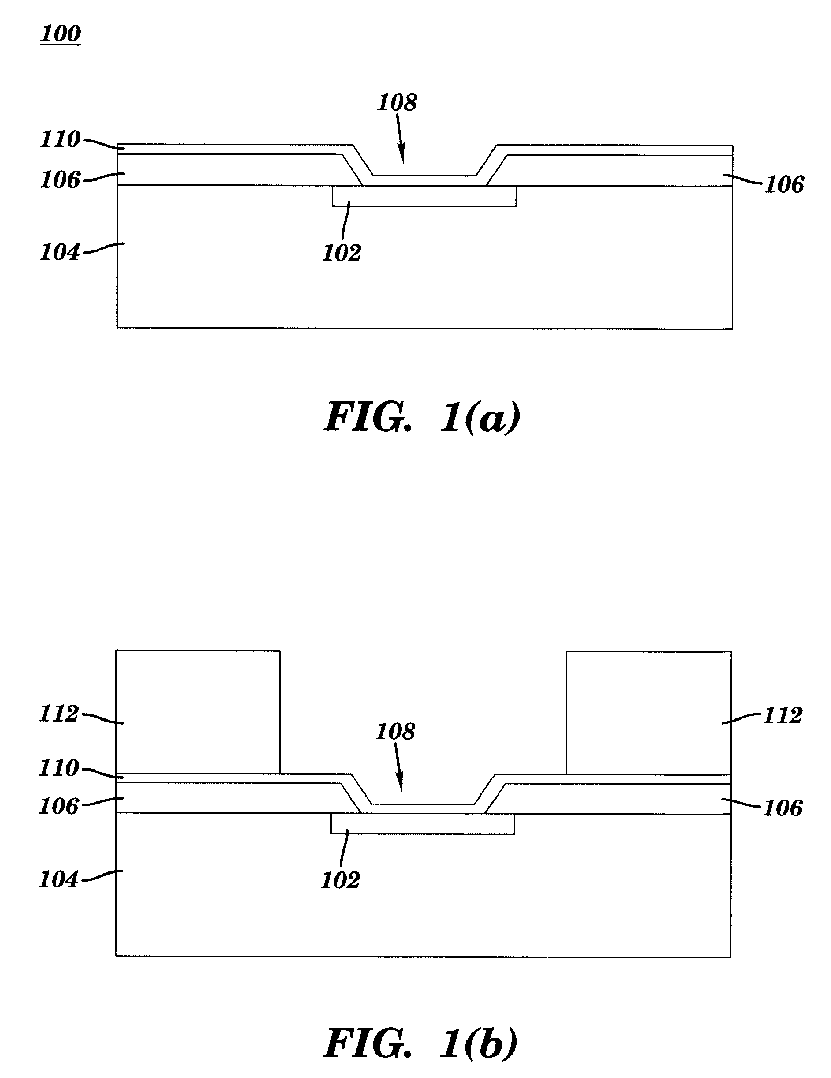
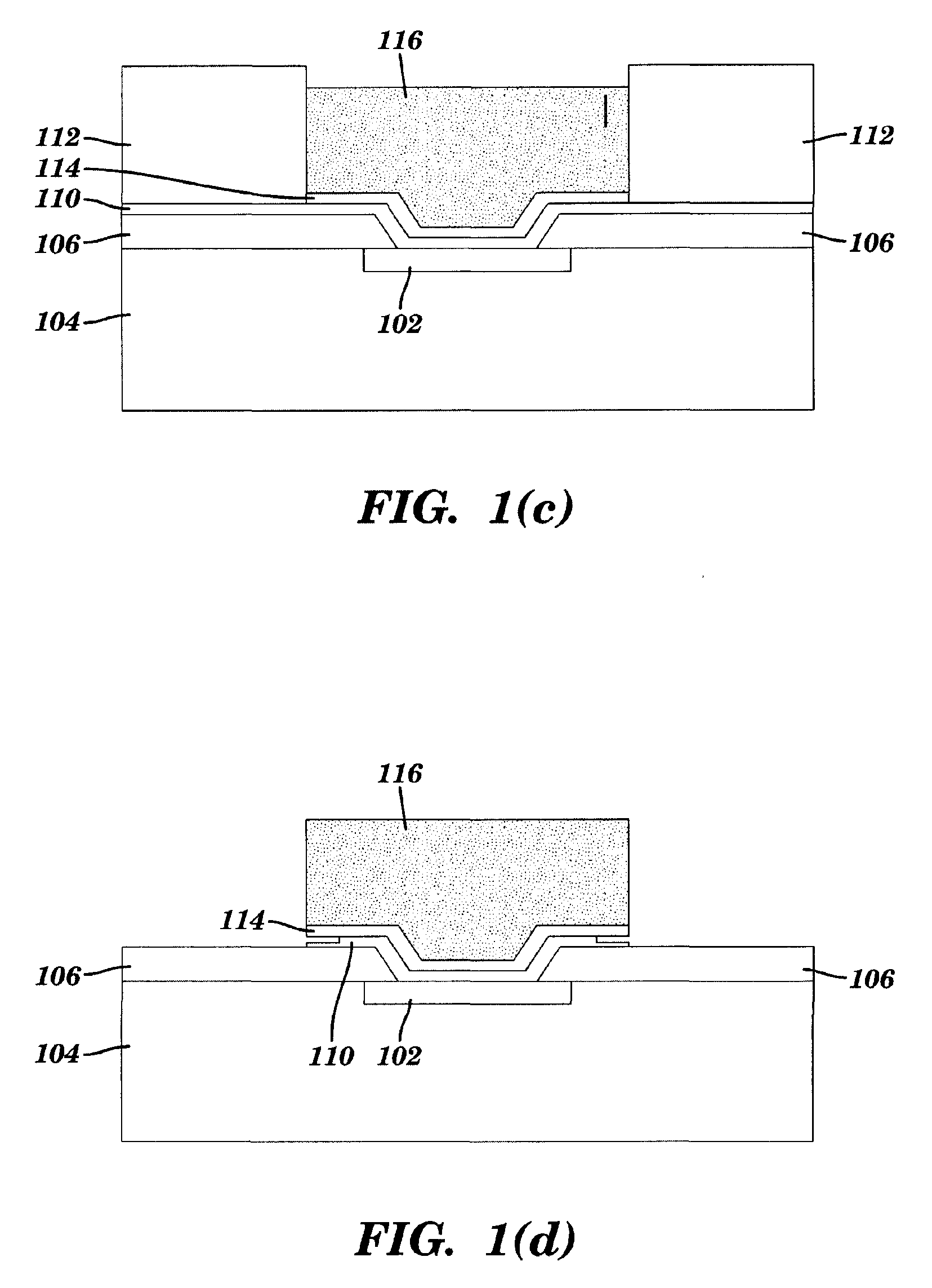
[0017] Disclosed herein is a method for forming robust solder interconnect structures by reducing effects of seed layer underetching with respect to a barrier layer. In one embodiment, an additional photolithography patterning step is used to separately define the areas in which the solder bump material is deposited, with respect to the patterning step used to define the areas for plating the barrier layer. The second patterning preferably results in a C4 pattern that is wider than the barrier layer pattern. In this manner, the subsequent etch of the seed layer results in an undercutting of the wider solder portions, and not the barrier layer itself. The wettablilty of the copper seed surface relative to the solder material results in a retraction of the solder to a truncated spherical shape upon reflow, with a complete BLM stack thereunderneath.

[0018] In another embodiment, the electrical resistivity and electrode potential of the Cu portion of the seed layer is altered by an anne...


PUM


Abstract

A method for forming an interconnect structure for a semiconductor device includes defining a via in a passivation layer so as expose a top metal layer in the semiconductor device. A seed layer is formed over the passivation layer, sidewalls of the via, and the top metal layer. A barrier layer is formed over an exposed portion of the seed layer, the exposed portion defined by a first patterned opening. The semiconductor device is annealed so as to cause atoms from the barrier layer to diffuse into the seed layer thereunderneath, wherein the annealing causes diffused regions of the seed layer to have an altered electrical resistivity and electrode potential with respect to undiffused regions of the seed layer.

Description

CROSS REFERENCE TO RELATED APPLICATIONS [0001] This application is a continuation of U.S. application Ser. No. 10 / 708,649, filed Mar. 17, 2004, the contents of which are incorporated herein in their entirety.BACKGROUND OF THE INVENTION [0002] The present invention relates generally to semiconductor device processing and, more particularly, to a method for forming robust solder interconnect structures by reducing effects of seed layer underetching with respect to a barrier layer. [0003] In the manufacture of semiconductor devices, C4 (Controlled-Collapse Chip Connection) is a means of connecting integrated circuit chips to substrates in electronic packages. In particular, C4 is a flip-chip technology in which the interconnections are small solder balls (or bumps) formed on the chip surface. The top layers of an integrated circuit chip include various wiring levels, separated by insulating layers of dielectric material, that provide input / output for the device. In C4 structures, the c...

Claims


Application Information

Patent Timeline
Patent Type & Authority Applications(United States)
IPC IPC(8): H01L21/44H01L21/48H01L23/485
CPCH01L24/10H01L2224/13099H01L24/13H01L2924/01013H01L2924/01022H01L2924/01029H01L2924/01074H01L2924/01078H01L2924/01082H01L2924/01322H01L2924/01327H01L2924/14H01L2924/19043H01L2924/01005H01L2924/01006H01L2924/01019H01L2924/01024H01L2924/01033H01L2924/014H01L2924/00H01L24/03H01L24/05H01L24/11H01L2224/0347H01L2224/0361H01L2224/03912H01L2224/05001H01L2224/05022H01L2224/05027H01L2224/0508H01L2224/05124H01L2224/05147H01L2224/05556H01L2224/05572H01L2224/05647H01L2224/05655H01L2224/1147H01L2224/13H01L2224/13006H01L2224/13007H01L2224/13027H01L2924/12042H01L2924/351Y02P80/30H01L2924/00014
Inventor SRIVASTAVA, KAMALESH K.SHINDE, SUBHASH L.CHENG, TIEN-JENKNICKERBOCKER, SARAH H.QUON, ROGER A.SABLINSKI, WILLIAM E.BIGGS, JULIE C.EICHSTADT, DAVID E.GRIFFITH, JONATHAN H.
Owner INVENSAS CORP
Why Eureka
Try Eureka