

Method of cutting processed object
a processing method and object technology, applied in the field of cutting objects, can solve the problems of unnecessary fractures, inability to perform precision cutting, and inability to cut accurately, so as to eliminate the action of pressing force and accurately be cut
- Summary
- Abstract
- Description
- Claims
- Application Information
AI Technical Summary
Benefits of technology
Problems solved by technology
Method used
Image

Examples
example 1
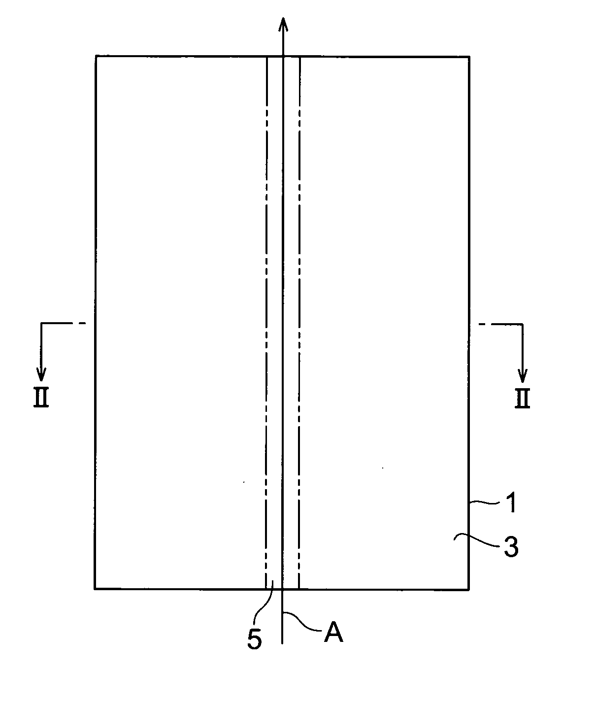
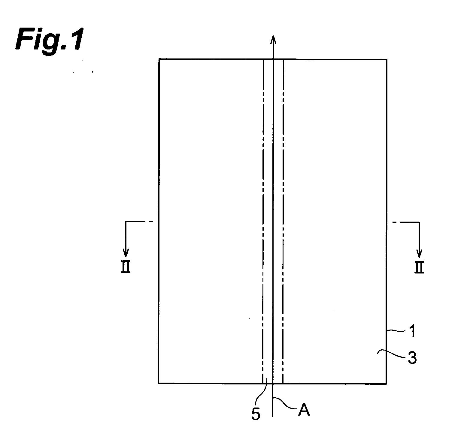
[0111] Example 1 of the method of cutting an object to be processed in accordance with the present invention will be explained. FIGS. 17, 18, and 22 to 24 are partial sectional views of the object to be processed 1 taken along the line XVII-XVII of FIG. 16. FIGS. 19 to 21 are partial sectional views of the object 1 taken along the line XIX-XIX of FIG. 16.
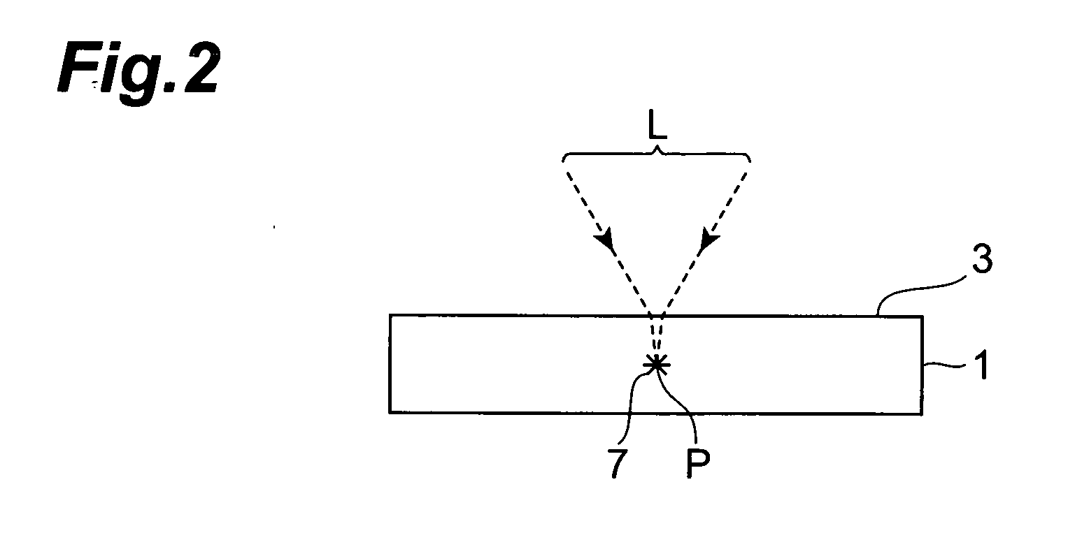
[0112] As shown in FIGS. 16 and 17, the front face 3 of the object to be processed 1, which is a silicon wafer, is formed with a plurality of functional devices 17 in a matrix in parallel with an orientation flat 16 of the object 1, whereby the object 1 is produced. Formed on the front face 3 side of the object 1 is an insulating film 18 made of SiO2 or the like, which covers the front face 3 and functional devices 17.
[0113] Therefore, the object 1 is a substrate, whereas the functional devices 17 and insulating film 18 constitute a laminate part disposed on the front face of the substrate. Here, the laminate part disposed on the ...
example 2
[0126] Example 2 of the method of cutting an object to be processed in accordance with the present invention will now be explained. FIGS. 25 to 27 are partial sectional views of the object 1 taken along the line XVII-XVII of FIG. 16.
[0127] As in Example 1 mentioned above, the object to be processed 1 shown in FIGS. 16 and 17 is produced, and a starting point region for cutting 8 is formed along a line along which the object should be cut 5 inside by a predetermined distance from the front face 3 (laser light incident face) of the object 1 (starting point region for cutting forming step). In the starting point region for cutting forming step in Example 2, the starting point region for cutting 8 shifted from the center line CL passing the center position of the object 1 in the thickness direction toward the rear face (one end face) 21 is formed along the line along which the object should be cut 5 as shown in FIG. 25.
[0128] Subsequently, as shown in FIG. 26, a protective film 20 is ...
PUM
| Property | Measurement | Unit |
|---|---|---|
| Moving speed | aaaaa | aaaaa |
| thickness | aaaaa | aaaaa |
| thickness | aaaaa | aaaaa |
Abstract
Description
Claims
Application Information