Package structure

a packaging and case technology, applied in the field of packaging structure, can solve the problems of increasing the complexity of the circuit board and the package case, the disadvantage of requiring a complex fabrication process, and the inability to effectively improve the production/assembly speed of the image sensing device, so as to reduce the noise interference and improve the sensing precision

Inactive Publication Date: 2010-07-22
PIXART IMAGING INC
View PDF6 Cites 58 Cited by
  • Summary
  • Abstract
  • Description
  • Claims
  • Application Information

AI Technical Summary

Benefits of technology

[0014]In the package structure of the present invention, the light emitting element and the light sensing element located on two sides of the substrate are separated from each other by the trench opened on the package layer, such that the lights generated...

Problems solved by technology

Therefore, the complexity in manufacturing the circuit board and the package case is increased, and the problem that the production/assembly speed of the image sensing device cannot be effectively improved still exists.
Therefore, the aforementioned package structure is still disad...

Method used


Image

  • Package structure
  • Package structure
  • Package structure

Examples


Embodiment Construction

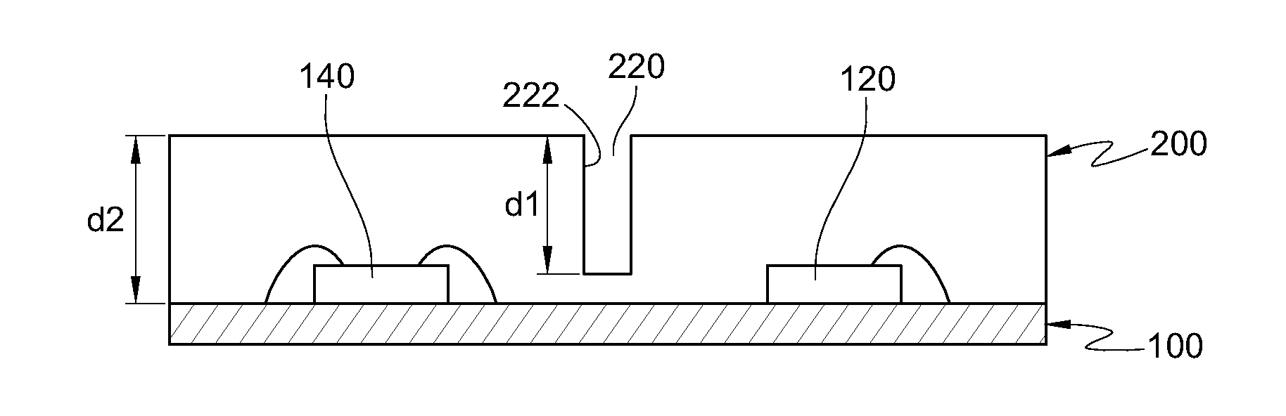
[0027]A package structure provided by the present invention is a modularized package structure of an image sensing device used in a digital camera, a biological recognition system, a fingerprint recognizer, an optical mouse, and other electronic products.

[0028]FIGS. 1 and 2 are respectively a schematic structural view and a schematic top view of a first embodiment of the present invention. The package structure according to the first embodiment of the present invention comprises a substrate 100 and a package layer 200. The substrate 100 is a conventional circuit board mounted with a circuit such as an integrated circuit board or a printed circuit board, or is a lead frame. A light emitting element 120 and a light sensing element 140 are disposed on the substrate 100, the light emitting element 120 is a light emitting diode (LED), a vertical cavity surface emitting laser (VCSEL), an edge-emitting laser (EELD), or other elements capable of emitting lights, and the light sensing elemen...


PUM


Abstract

A package structure is described. A light emitting element and a light sensing element are disposed on a substrate, and are both wrapped by a package layer. Meanwhile, the light emitting element and the light sensing element are separated by a trench of the package layer, such that lights generated by the light emitting element are blocked, thereby reducing the noise interference on the light sensing element and improving the sensing precision of the light sensing element.

Description

CROSS-REFERENCE TO RELATED APPLICATIONS[0001]This non-provisional application claims priority under 35 U.S.C. § 119(a) on Patent Application No(s). 098201189 filed in Taiwan, R.O.C. on Jan. 21, 2009 the entire contents of which are hereby incorporated by reference.BACKGROUND OF THE INVENTION[0002]1. Field of Invention[0003]The present invention relates to a package structure, in particular, to a package structure having a light source and a light source sensor integrated on a circuit board.[0004]2. Related Art[0005]With the rapid development of electronic technology, image sensing has been more and more widely applied, for example, in a digital camera, a biological recognition system, a fingerprint recognizer, an optical mouse, and other electronic products.[0006]In a package structure generally utilized in an image sensing device, the mainly required elements are modularized to facilitate the assembly of the image sensing device in production. The package structure substantially in...

Claims


Application Information

Patent Timeline
IPC IPC(8): H01L31/12H01L31/0203
CPCH01L31/0203H01L31/153H01L2224/48227H01L2224/49175H01L2924/1815H01L2224/48091H01L2924/00014H01L2924/181H01L2924/00H01L2924/00012
Inventor LI, KUO-HSIUNGCHEN, HUI-HSUAN
Owner PIXART IMAGING INC
Why Eureka
Try Eureka