Organic light emitting element, display device including the same and method for manufacturing organic light emitting element

a technology of organic light emitting elements and display devices, which is applied in the direction of discharge tubes/lamp details, organic semiconductor devices, discharge tubes/lamp details, etc., can solve the problems of high drive voltage, inability to apply uniform voltage to the second electrode, and inability to perform image display with high uniformity, etc., to achieve the effect of high luminance and image display

Active Publication Date: 2006-01-26
GLOBAL OLED TECH
View PDF12 Cites 102 Cited by
  • Summary
  • Abstract
  • Description
  • Claims
  • Application Information

AI Technical Summary

Benefits of technology

[0019] The present invention has been achieved in view of the above problems. An object of the present invention is to provide an organic EL element which allows image display with high luminance without causing variations in luminance.

Problems solved by technology

As a result, a high drive voltage is required.
Therefore, a uniform voltage cannot be applied to the second electrode made of the highly resistive, transparent conductive material.
This leads to a problem in that image display cannot be performed with high uniformity.

Method used


Image

  • Organic light emitting element, display device including the same and method for manufacturing organic light emitting element
  • Organic light emitting element, display device including the same and method for manufacturing organic light emitting element
  • Organic light emitting element, display device including the same and method for manufacturing organic light emitting element

Examples


embodiment 1

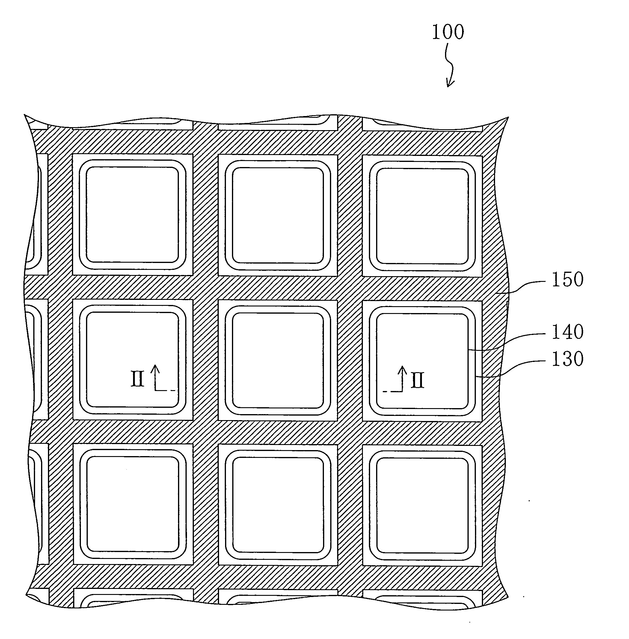
[0048]FIG. 1 is a schematic plan view illustrating an organic EL element 100 of Embodiment 1.

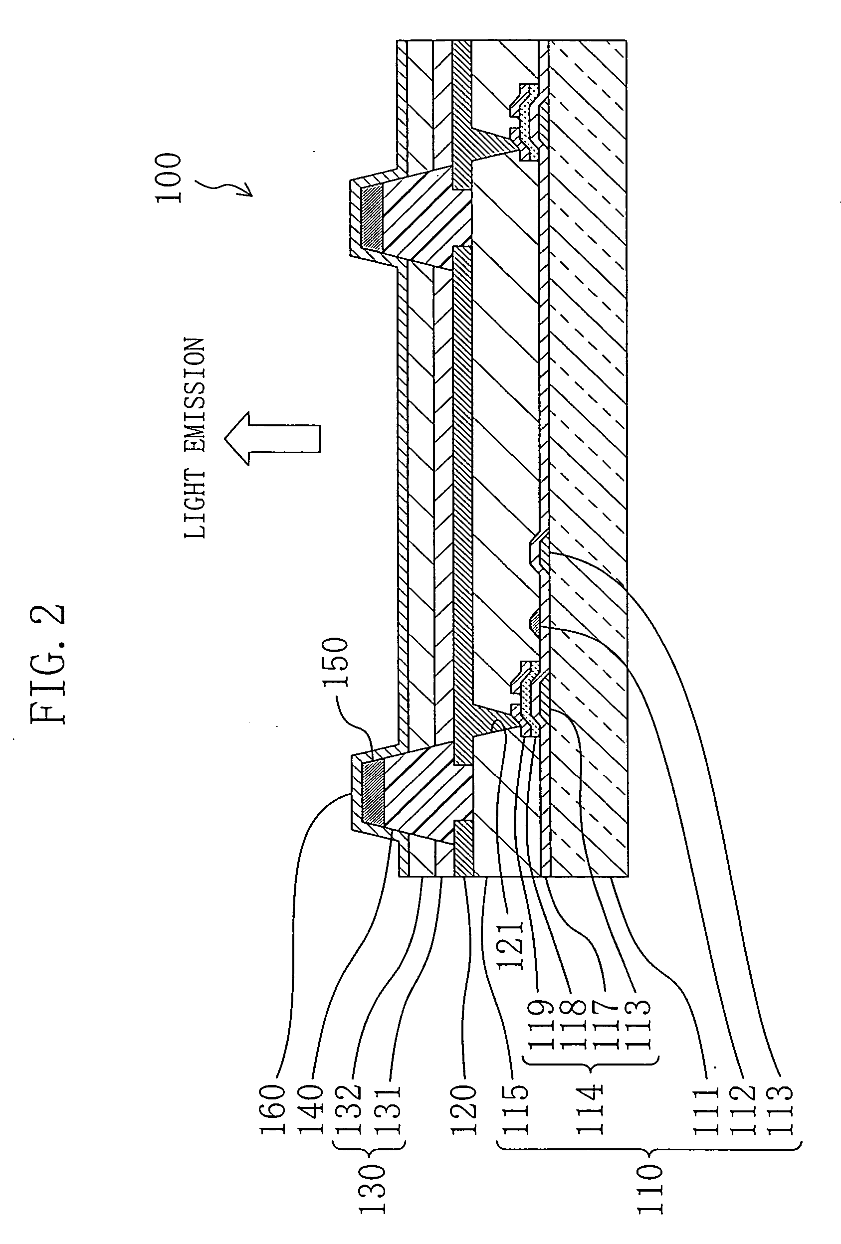
[0049]FIG. 2 is a schematic sectional view taken along the line II-II shown in FIG. 1.

[0050] The organic EL element 100 includes a thin film transistor (TFT) substrate 110, a plurality of first electrodes 120 which are arranged on the TFT substrate 110 in a predetermined configuration (e.g., a matrix configuration), a wall-like insulating layer 140 which isolates the first electrodes 120 from each other, organic light emitting layers 130 formed on the first electrodes 120, respectively, an auxiliary electrode 150 formed on the wall-like insulating layer 140 and a second electrode 160 which is formed to cover the surfaces of the wall-like insulating layer 140, the auxiliary electrode 150 and the organic light emitting layers 130 and electrically connected to the auxiliary electrode 150. The second electrode 160 is transparent to light emitted from the organic light emitting layer 130. For t...

embodiment 2

[0102] An organic EL element 200 of Embodiment 2 is substantially the same as the organic EL element 100 of Embodiment 1 except where to provide the auxiliary electrode and the structure of the pixels. Now, with reference to the drawings, a detailed explanation is given of where to provide the auxiliary electrode and the structure of pixels P in the organic EL element 200 of Embodiment 2.

[0103]FIG. 10 is a plan view illustrating the organic EL element 200 of Embodiment 2.

[0104] The organic EL element 200 includes organic light emitting layers 230B for emitting blue (B) light, organic light emitting layers 230R for emitting red (R) light and organic light emitting layers 230G for emitting green (G) light. Among the organic light emitting layers 230B, 230R and 230G, the organic light emitting layers 230B have the largest light emitting area, while the organic light emitting layers 230G have the smallest light emitting area. The light emitting area of the organic light emitting layer...

embodiment 3

[0109] An organic EL element 300 of Embodiment 3 is substantially the same as the organic EL element 100 of Embodiment 1 except where to provide the auxiliary electrode and the structure of the pixels. Now, with reference to the drawings, a detailed explanation is given of where to provide the auxiliary electrode and the structure of pixels P in the organic EL element 300 of Embodiment 3.

[0110]FIG. 11 is a plan view illustrating the organic EL element 300 of Embodiment 3.

[0111] The organic EL element 300 includes organic light emitting layers 330B for emitting blue light, organic light emitting layers 330R for emitting red light and organic light emitting layers 330G for emitting green light. Among the organic light emitting layers 330B, 330R and 330G, the organic light emitting layers 330B have the largest light emitting area, while the organic light emitting layers 330G have the smallest light emitting area. The light emitting area of the organic light emitting layers 330R is sm...


PUM


Abstract

An organic EL element includes a substrate, a plurality of first electrodes which are arranged on the substrate in a matrix configuration, a wall-like insulating layer which is formed on the substrate, organic light emitting layers which are formed on the first electrodes, respectively, an auxiliary electrode which is formed on top of the wall-like insulating layer and a second electrode which is formed to cover the surfaces of the wall-like insulating layer, the auxiliary electrode and the light emitting layers and electrically connected to the auxiliary electrode. The second electrode is transparent to light from the light emitting layers.

Description

CROSS-REFERENCE TO RELATED APPLICATION [0001] This non-provisional application claims priority under 35 U.S.C. §119(a) on Patent Applications Nos. 2004-214491 filed in Japan on Jul. 22, 2004 and 2005-92088 filed in Japan on 28 Mar. 2005, the entire contents of which are hereby incorporated by reference. BACKGROUND OF THE INVENTION [0002] (a) Field of the Invention [0003] The present invention relates to an organic light emitting element, a display device including the same and a method for manufacturing the organic light emitting element. [0004] (b) Description of Related Art [0005] As compared with conventionally used cathode ray tube (CRT) display elements, flat display elements are more power-saving and slimmed down. As a wide variety of information processing apparatuses have been developed in recent years, there is a growing demand for the flat display elements. Examples of the flat display elements include, for example, liquid crystal display elements and electroluminescent di...

Claims


Application Information

Patent Timeline
Patent Type & Authority Applications(United States)
IPC IPC(8): H05B33/00
CPCH01L27/3246H01L51/5228H01L27/3279H01L2251/5315H01L51/5234H10K59/122H10K59/1315H10K50/824H10K50/828H10K2102/3026H05B33/26H05B33/10
Inventor NOGUCHI, NOBORUTAGAWA, AKIRA
Owner GLOBAL OLED TECH
Why Eureka
Try Eureka