Semiconductor integrated circuit

a technology of integrated circuits and semiconductors, applied in pulse generators, instruments, pulse techniques, etc., can solve problems such as lsi breakdown and operation failure, diodes not necessarily providing a suitable structure, and generate catchup phenomena, etc., to achieve the effect of higher ra

Inactive Publication Date: 2006-02-02
SOCIONEXT INC
View PDF5 Cites 3 Cited by
  • Summary
  • Abstract
  • Description
  • Claims
  • Application Information

AI Technical Summary

Benefits of technology

[0007] Therefore, a main object of the present invention is to prevent the generation of the latchup phenomenon when the substrate of the MOS transistor is subjected to the forward bias in order to attain an operation at a higher rate. A semiconductor integrated circuit according to the present invention comprises an MOS substrate having a substrate region (MOS) and a source region separated from each other, a dummy MOS circuit substrate-separated from the MOS circuit and having a substrat

Problems solved by technology

In a CMOS transistor, there is a possibility that a latchup phenomenon is generated when a noise is applied in the state in which a substrate bias voltage is applied in a forward direction (forward bias).
The generation of the latchup phenomenon results in LSI breakdown and operation failure.
Therefore

Method used


Image

  • Semiconductor integrated circuit
  • Semiconductor integrated circuit
  • Semiconductor integrated circuit

Examples


Embodiment Construction

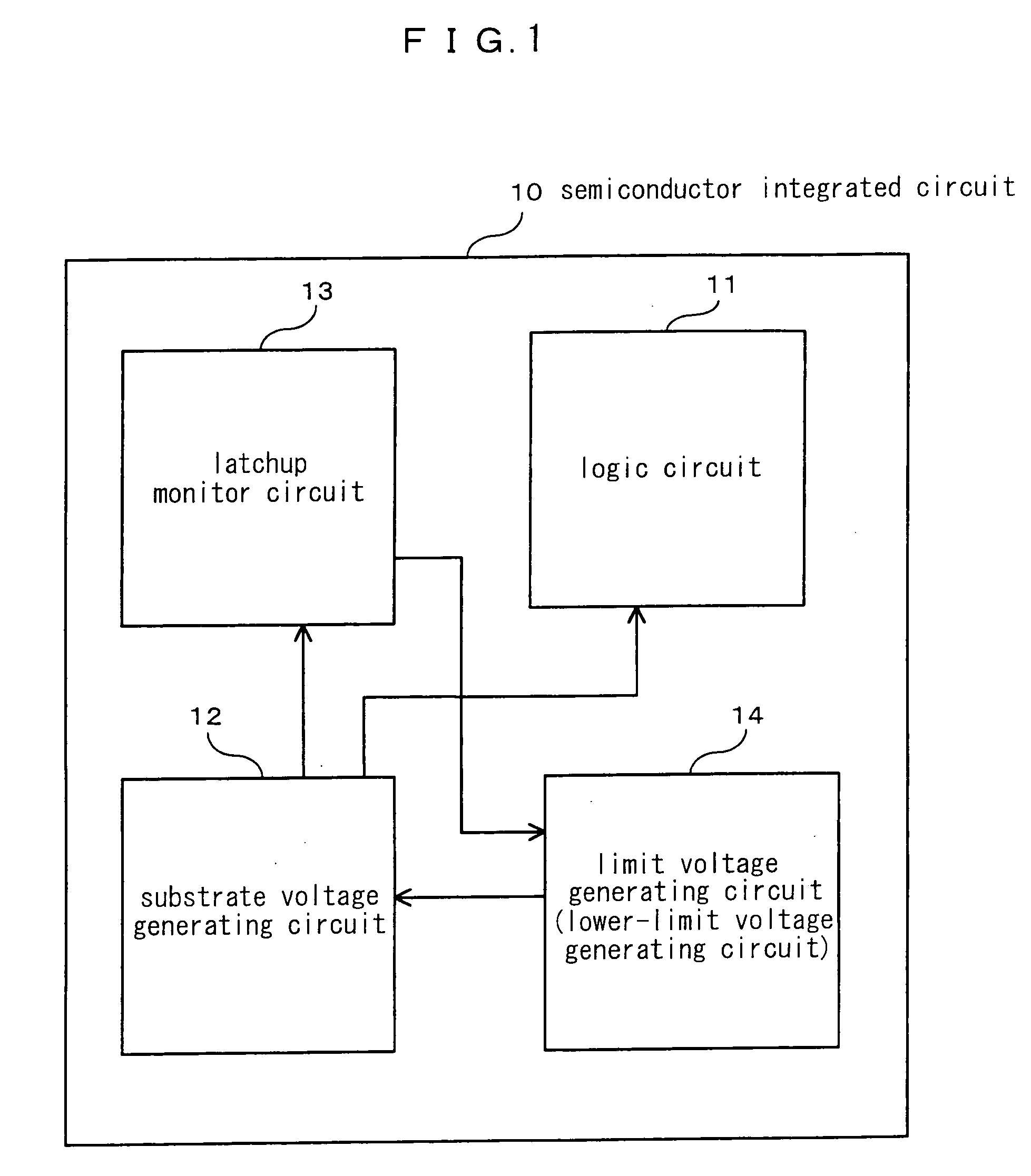
[0030] Hereinafter, a preferred embodiment of the present invention is described referring to the drawings. FIG. 1 is a block diagram illustrating a constitution of a semiconductor integrated circuit 10 according to the preferred embodiment.

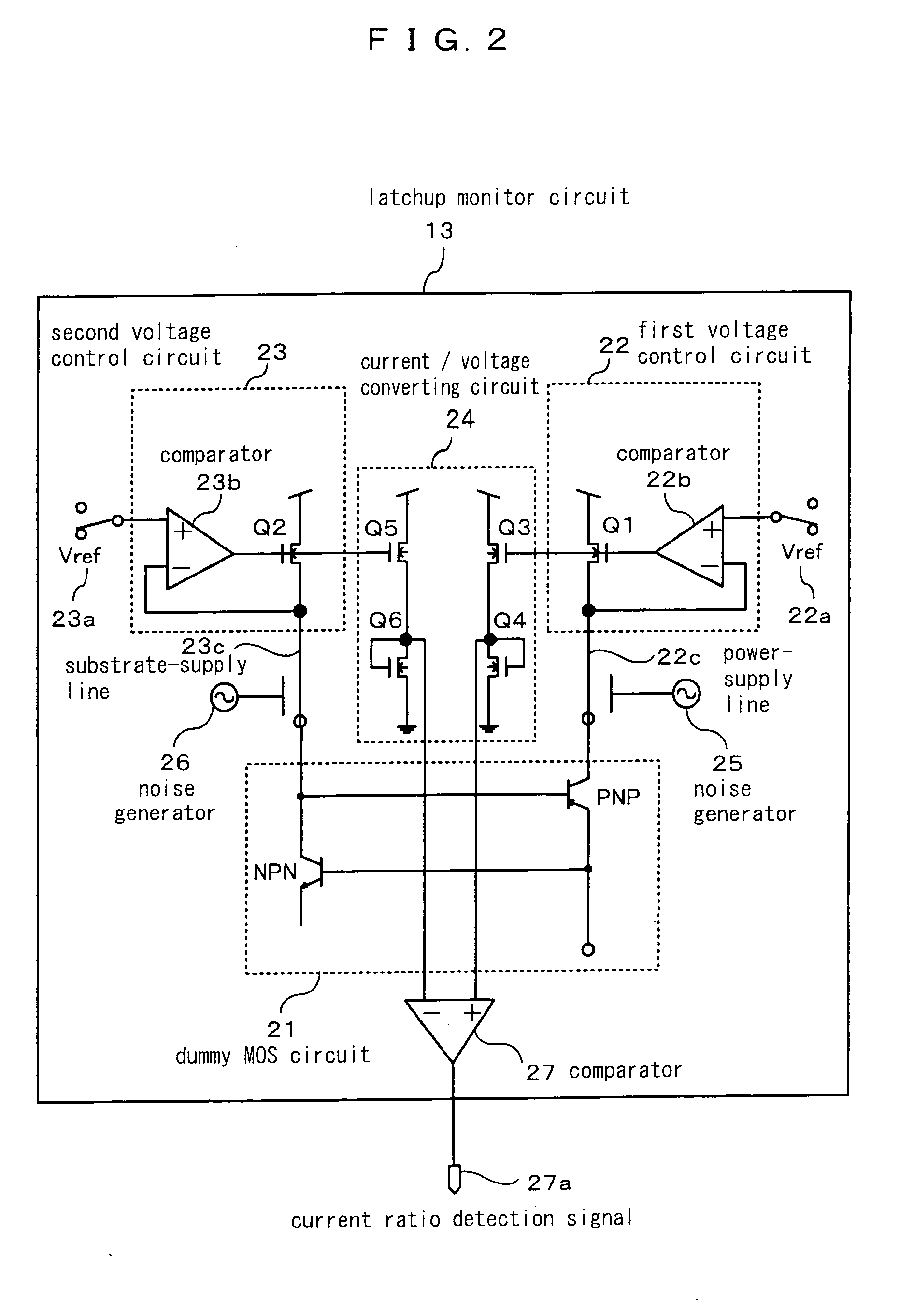
[0031] The semiconductor integrated circuit 10 comprises a logic circuit 11 for realizing a function, a substrate voltage generating circuit 12, a latchup monitor circuit 13 and a limit voltage generating circuit 14.

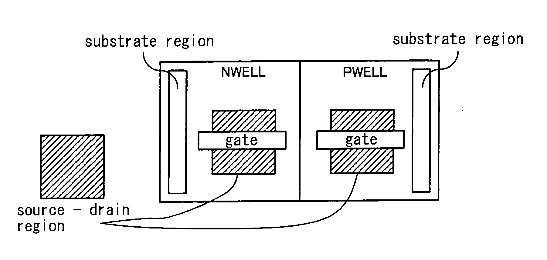
[0032] The substrate voltage generating circuit 12 supplies a substrate voltage to a substrate of a PMOS transistor or an NMOS transistor in an MOS circuit to be controlled in the logic circuit 11. The latchup monitor circuit 13 monitors a reference voltage supplied to the MOS circuit of the logic circuit 11 from the substrate voltage generating circuit 12. The limit voltage generating circuit 14 controls a limit value of a forward-bias voltage of the substrate voltage generating circuit 12.

[0033] The limit voltage generating circu...


PUM


Abstract

A semiconductor integrated circuit according to the present invention comprises an MOS substrate having a substrate region (MOS) and a source region separated from each other, a dummy MOS circuit substrate-separated from the MOS circuit and having a substrate region (dummy) and a source region (dummy) separated from each other, a substrate voltage generating circuit for generating a substrate voltage to be applied to the substrate region (MOS) and the substrate region (dummy), and a comparing circuit for measuring a current generated in the dummy MOS substrate, wherein an area ratio between the substrate region (dummy) and the source region (dummy) is substantially equal to an area ratio between the substrate region (MOS) and the source region (MOS).

Description

BACKGROUND OF THE INVENTION [0001] 1. Field of the Invention [0002] The present invention relates to a semiconductor integrated circuit, more particularly to a technology for controlling a substrate voltage applied to an MOS (Metal Oxide Semiconductor) transistor in which a source and a substrate are separated from each other. [0003] 2. Description of the Related Art [0004] In a CMOS transistor, there is a possibility that a latchup phenomenon is generated when a noise is applied in the state in which a substrate bias voltage is applied in a forward direction (forward bias). To describe the latchup phenomenon, a parasitic bipolar transistor (thyristor structure) remains a conducted state, in which a large current flow is constantly generated between a power-supply terminal and a ground terminal. The generation of the latchup phenomenon results in LSI breakdown and operation failure. [0005] As a conventional method for preventing the generation of the latchup phenomenon, as shown in ...

Claims


Application Information

Patent Timeline
IPC IPC(8): H01L29/78
CPCH01L27/0207H03K19/00315H01L27/0921
Inventor SUMITA, MASAYA
Owner SOCIONEXT INC
Why Eureka
Try Eureka