

Cap wafer, semiconductor package, and fabricating method thereof
a technology of semiconductor packaging and cap wafer, which is applied in the direction of semiconductor devices, semiconductor/solid-state device details, electrical apparatus, etc., can solve the problems of limiting the number of devices, affecting the yield of packaging, and affecting the performance of chip performance, so as to reduce the size of the device, the effect of improving the packaging yield
- Summary
- Abstract
- Description
- Claims
- Application Information
AI Technical Summary
Benefits of technology
Problems solved by technology
Method used
Image

Examples
Embodiment Construction
[0052] Certain embodiments of the present invention will be described in greater detail with reference to the accompanying drawings.
[0053] In the following description, the same drawing reference numerals are used for the same elements shown in different drawings. The following detailed description as to construction and structural elements are provided to assist in a comprehensive understanding of the invention. However, the present invention should not be construed as being limited thereto. Also, well-known functions or constructions are not described in detail since they would obscure the invention in unnecessary detail.
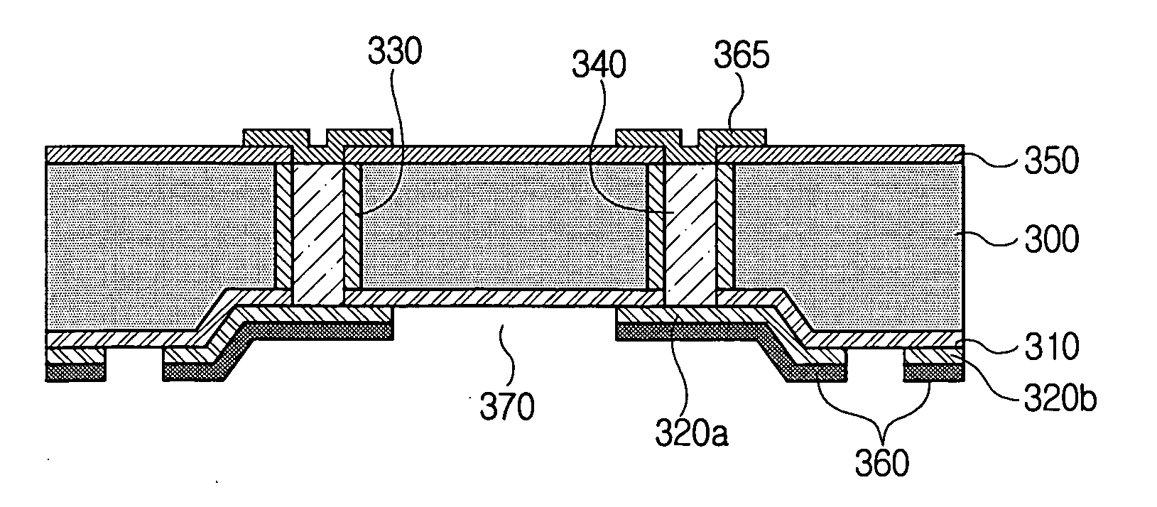
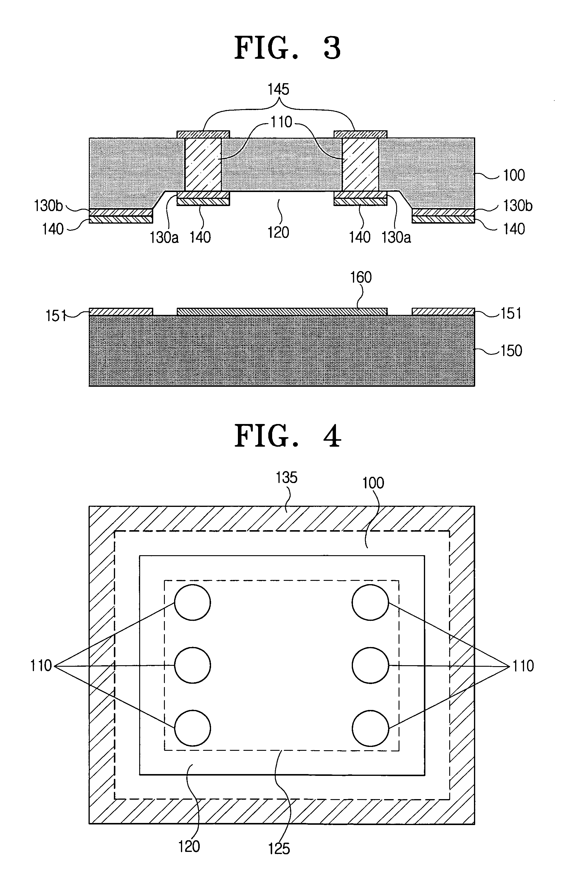
[0054]FIG. 3 is a vertical cross-sectional view of a cap wafer according to an embodiment of the present invention and a packaged semiconductor device fabricated using the cap wafer. Referring to FIG. 3, a cap wafer 100 includes a feed-through 110, a cavity 120, an upper electrode 145, a lower electrode 130a, a pad 130b, and a first sealing layer 140. As shown i...
PUM
 Abstract
Description
Claims
Application Information