Integration circuit, decrement circuit, and semiconductor devices

a technology of integrated circuits and decrements, applied in the field of circuit technology for semiconductor devices, can solve the problems of limited devices, difficult mounting of easy-to-use digital cmos circuits together with other circuits, etc., and achieve the effect of reducing the size and the area of circuitry

Inactive Publication Date: 2006-02-02
RENESAS ELECTRONICS CORP
View PDF7 Cites 30 Cited by
  • Summary
  • Abstract
  • Description
  • Claims
  • Application Information

AI Technical Summary

Benefits of technology

[0011] It is therefore an object of the invention to provide an ignitor in which the size and area of circuits with millisecond-order time constants are minimized and which can be automatically shut down upon detection of an abnormality without causing erroneous ignition.
[0019] In accordance with the invention, an integration circuit of millisecond order can be constructed of only a diode and a capacitor by utilizing the reverse leak resistance of the diode. Therefore, the size and area of circuitry can be decreased as compared with cases where digital circuits are used.
[0020] Further, when the invention is applied to an ignitor, an integration circuit of millisecond order can be realized on the same semiconductor chip as a switching device. As a result, an ignition system that does not lead to erroneous ignition upon self-shutdown can be realized.

Problems solved by technology

Consequently, available devices are limited, and it is not easy to mount an easy-to-use digital CMOS circuit together with other circuits.

Method used


Image

  • Integration circuit, decrement circuit, and semiconductor devices
  • Integration circuit, decrement circuit, and semiconductor devices
  • Integration circuit, decrement circuit, and semiconductor devices

Examples


embodiment 1

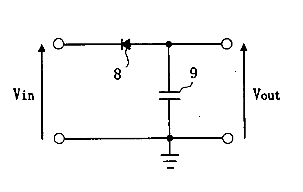
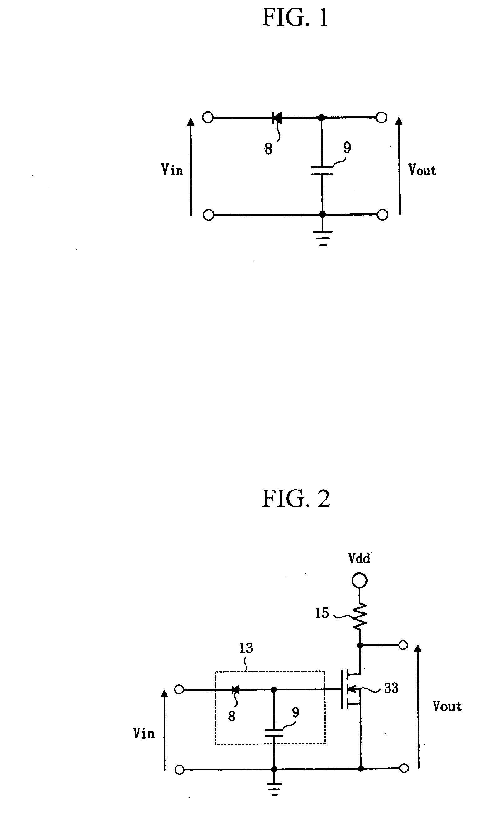
[0035]FIG. 1 shows the circuit diagram of an example of an integration circuit according to an embodiment of the invention.

[0036] The integration circuit of the present embodiment comprises a diode 8 and a capacitor 9 that are connected in series between an input terminal (Vin) and ground. The cathode of the diode 8 functions as the input terminal. The anode of the diode 8 is connected to one end of the capacitor 9 to function as an output terminal (Vout). The other end of the capacitor 9 is connected to ground. Although conventional RC integration circuits consist of a resistor and a capacitor connected in series, the resistor element is characteristically replaced with a diode in accordance with the invention.

[0037] The reverse leak resistance of the diode 8 is on the order of several megaohms to several gigaohms, so that a high-value resistor can be fabricated on the semiconductor substrate within a small area. When the reverse leak resistance of the diode 8 is designed to be 1...

embodiment 2

[0040]FIG. 2 shows the circuit diagram of a decrement circuit in accordance with a second embodiment of the invention.

[0041] The decrement circuit of the present embodiment comprises an integration circuit 13, a resistor 15, and a MOSFET 33. The resistor 15 and the MOSFET 33 are connected in series between a power supply terminal (Vdd) and ground. The point of connection of the resistor 15 and the MOSFET 33 is used as an output terminal (Vout), with the output of the integration circuit 13 being connected to the gate of the MOSFET 33. The integration circuit 13 is the same circuit as described with reference to Embodiment 1.

[0042] In this decrement circuit, the MOSFET 33, which is of N-type, has its drain connected to the resistor 15, with the point of connection being used as the output terminal. The gate of the MOSFET 33 is connected to the output of the integration circuit 13. In this decrement circuit, the gate voltage of the MOSFET 33 is incremented by the integration circuit...

embodiment 3

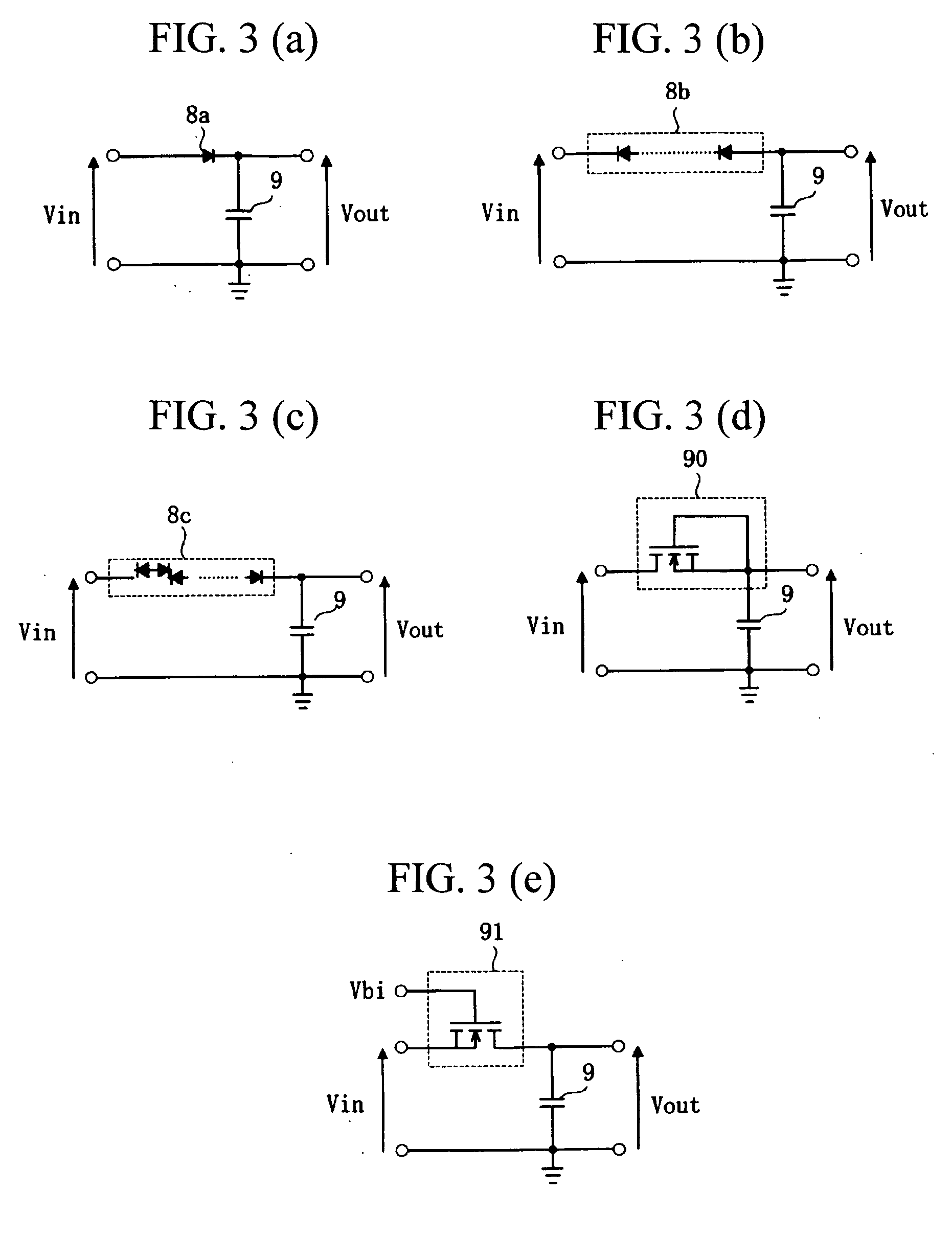
[0044]FIG. 3 shows circuit diagrams of other examples of the integration circuit of the invention.

[0045]FIG. 3(a) shows an integration circuit for obtaining an increased time constant during the fall transition of the input signal. The example differs from the circuit shown in FIG. 1 in that the diode 8a is disposed in the opposite direction. Namely, the anode of the diode 8a is connected to the input side, and the cathode is connected to the capacitor 9. In this way, the capacitor 9 can be slowly discharged during the fall transition of the input signal.

[0046]FIG. 3(b) shows another example in which a plurality of diodes 8b are connected in series. In this way, the time constant of the integration circuit can be increased.

[0047]FIG. 3(c) shows another example in which a plurality of diodes 8c are connected in alternating directions to form the so-called back-to-back connection. In this connection, the anodes or cathodes of adjacent diodes 8c can be commonly utilized, so that the...


PUM


Abstract

An ignitor comprising a circuit with a millisecond order time constant and with a minimum circuit size and area, which is capable of self-shutdown without leading to erroneous ignition upon detection of an abnormality. An ignitor 1 capable of self-shutdown upon detection of an abnormality comprises an abnormality detection circuit 12 whose rise output is applied to the gate of a self-shutdown MOSFET 33 via an integration circuit 33 comprised of a diode 8 and a capacitor 9. The gate voltage of IGBT 5a, which is a main-current switching device, can be decremented.

Description

BACKGROUND OF THE INVENTION [0001] 1. Field of the Invention [0002] The present invention relates to a circuit technology for semiconductor devices. Particularly, it relates to a technology that can be effectively applied to a semiconductor device with components that can be fabricated on a semiconductor substrate chip, including an integration circuit with a time constant on the millisecond order, a decrement circuit, and a semiconductor device with a soft shutting-down function. The invention also relates to an ignition device (to be hereafter referred to as “an ignitor”) for automotive engines to which the semiconductor device is applied. [0003] 2. Background Art [0004] The following is an analysis of ignitors for automotive engines conducted by the inventors. [0005] As ignitors for automotive engines, distributorless ignition systems are increasingly replacing the conventional distributor-employing systems for the purpose of saving energy. In the distributorless ignition systems...

Claims


Application Information

Patent Timeline
Patent Type & Authority Applications(United States)
IPC IPC(8): F02P15/00F02P3/04
CPCF02P3/0552
Inventor YUKUTAKE, SEIGOUMORI, MUTSUHIROKOHNO, YASUHIKO
Owner RENESAS ELECTRONICS CORP
Why Eureka
Try Eureka