Image capturing device

a technology image, which is applied in the field of image capturing device, can solve the problems of increasing the size of the chip, working against the size reduction affecting the optical characteristics, so as to reduce the size prevent the displacement of the transparent member, and improve the reliability and optical characteristics of the image capturing devi

Inactive Publication Date: 2006-02-02
SOCIONEXT INC
View PDF12 Cites 84 Cited by
  • Summary
  • Abstract
  • Description
  • Claims
  • Application Information

AI Technical Summary

Benefits of technology

[0014] Accordingly, it is a general object of the present invention to provide an image capturing device in which the above-described disadvantages are eliminated.
[0015] A more specific object of the present invention is to provide an image capturing device having a transparent member such as a glass plate provided on the light receiving surface of an image capturing element, in which the displacement of the transparent member and the entrance of unnecessary light into the light receiving part of the image capturing element can be prevented while the image capturing device is reduced in size.
[0017] According to the above-described image capturing device, a plate-like transparent member is provided on the light receiving surface of a light receiving element, and the first principal plane of the transparent member positioned on the light receiving element side is greater in area than the second principal plane thereof (outer surface) opposite the first principal plane. According to this configuration, the displacement of the transparent member can be prevented, and the entrance of unnecessary light can be controlled. As a result, the reliability and the optical characteristics of the image capturing device can be improved. Further, it is possible to reduce the size of the image capturing device while preventing interference with a bonding capillary in its manufacturing process.

Problems solved by technology

When the unnecessary light enters the light receiving surface, optical characteristics are impaired, thus causing a flare or ghost.
However, if the glass plate, the light transmitting substrate, or the light transmitting member is reduced in size, light reflected by its end faces is likely to enter an image-capturing area so as to hinder optical characteristics.
On the other hand, an increase in chip size works against the size reduction of image capturing devices.

Method used


Image

  • Image capturing device
  • Image capturing device
  • Image capturing device

Examples


first embodiment

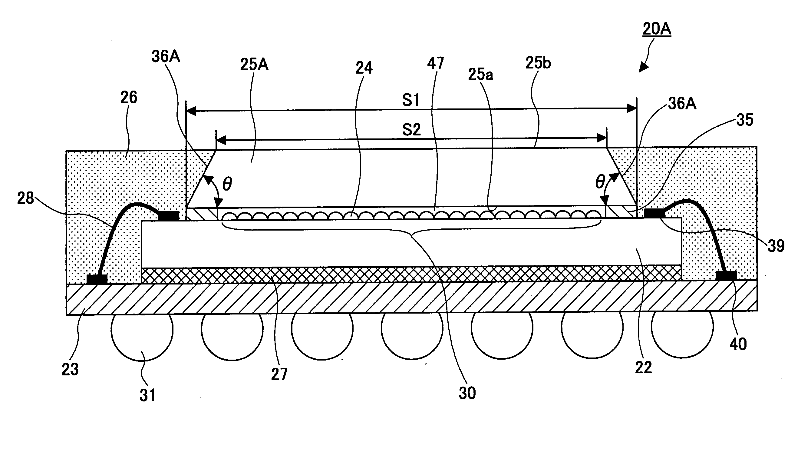
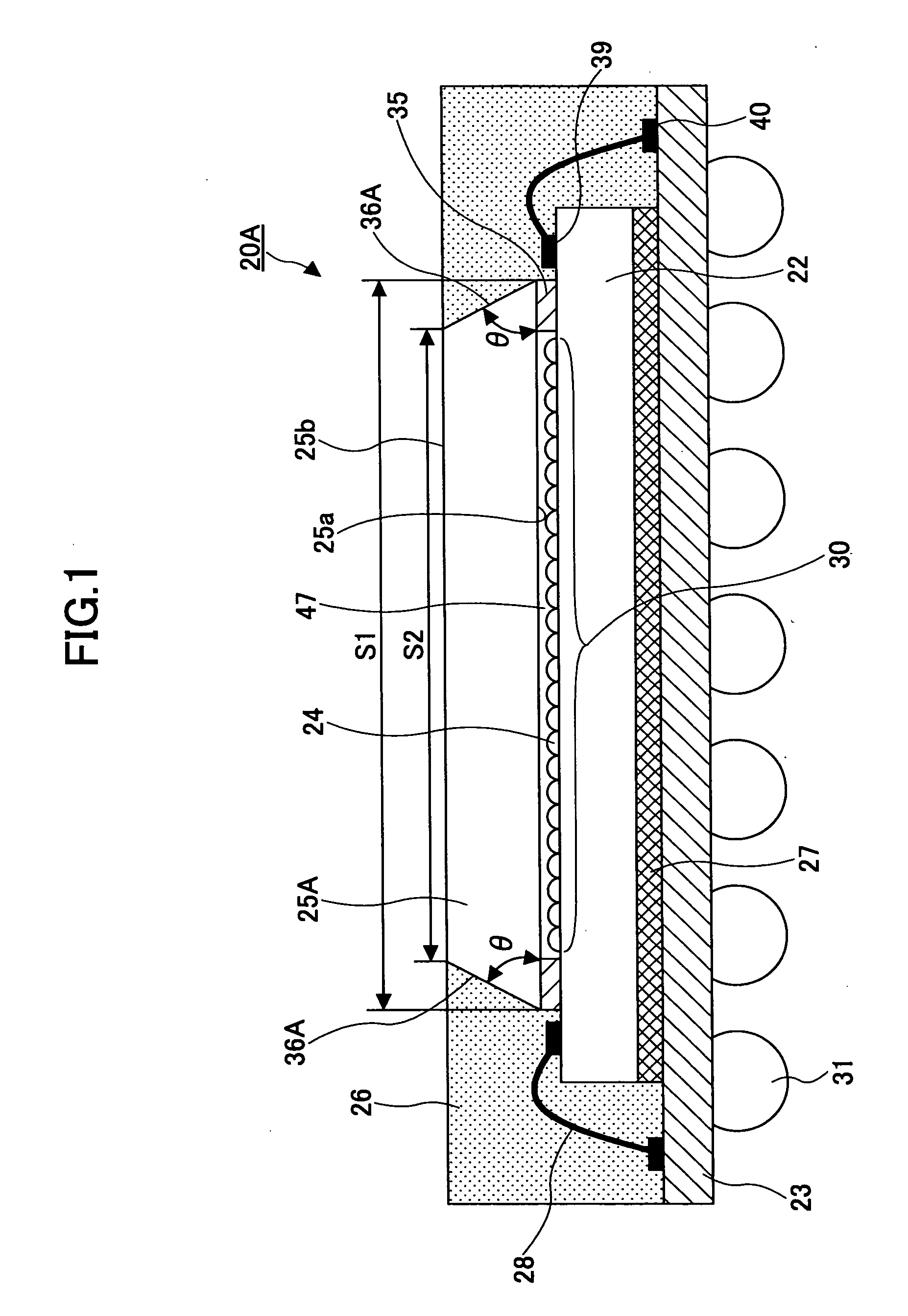
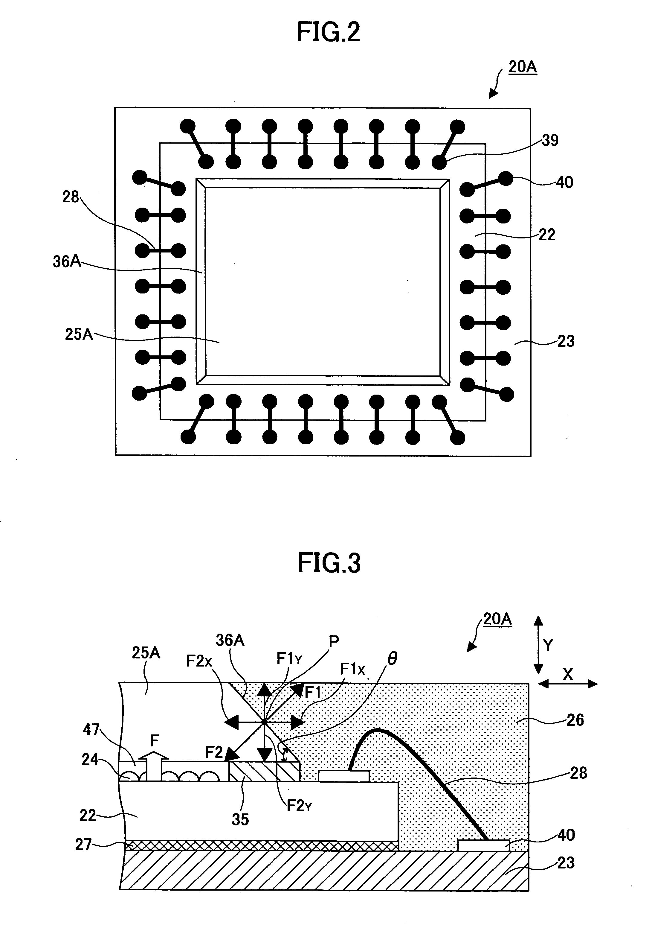
[0036]FIGS. 1 and 2 shows an image capturing device 20A, which is the image capturing device according to the present invention. FIG. 1 is a cross-sectional view of the image capturing device 20A. FIG. 2 is a plan view of the image capturing device 20A from which sealing resin 26 is removed.

[0037] In this embodiment, the image capturing device 20A includes an image capturing element (light receiving element) 22, a support substrate 23, a microlens 24, a plate-like transparent member 25A, the sealing resin 26, and external connection terminals 31. The image capturing element 22, which is composed of a CMOS image sensor, is mounted on and adhered to the support substrate 23 via a die bonding material 27 with a light receiving surface 30 of the image capturing element 22 facing upward.

[0038] Multiple photodiodes are formed in a matrix-like manner (not graphically represented) on the light receiving surface 30 (the image capturing area) of the image capturing element 22. The microlens ...

second embodiment

[0058] Next, a description is given below, with reference to FIGS. 6 and 7, of the image capturing device according to the present invention.

[0059]FIG. 6 is a cross-sectional view of an image capturing device 20B according to the second embodiment. In FIG. 6, the same elements as those described in the first embodiment are referred to by the same numerals, and a description thereof is omitted. The same applies to the drawings of the below-described other embodiments.

[0060] As shown enlarged in FIG. 7, in the image capturing device 20B according to the second embodiment, a side surface 36B of a transparent member 25B is roughened. As in the above-described first embodiment, the side surface 36B of the transparent member 25B is inclined. The side surface 36B of the transparent member 25B is roughened. As a result, of light entering the transparent member 25B, light reaching the side surface 36B is scattered, so that the amount of light entering the light receiving surface 30 (image c...

third embodiment

[0062] Next, a description is given of the image capturing device according to the present invention.

[0063]FIG. 8 is a cross-sectional view of an image capturing device 20C according to the third embodiment. In the image capturing device 20C according to the third embodiment, a flange part 56 is provided on the side surface 36A of a transparent member 25C on its first principal plane 25a side. In the transparent member 25C, the first principal plane 25a positioned on the image capturing element 22 side is also greater in area than the second principal plane 25b positioned on the outer side, and an acute angle θ is also formed between the side surface 36A and the first principal plane 25a. The provision of the flange part 56 substantially increases the area of contact of the transparent member 25C and the sealing resin 26.

[0064] The flange part 56 is provided on the first principal plane 25a side. As a result, in the resin sealing structure, the flange part 56 produces the so-called...


PUM


Abstract

An image capturing device is disclosed that includes a light receiving element having a light receiving surface, a plate-like transparent member provided on the light receiving surface of the light receiving element, and resin provided to at least the periphery of the plate-like transparent member. The plate-like transparent member includes a first principal plane positioned on the light receiving element side and a second principal plane opposite the first principal plane. The first principal plane is greater in area than the second principal plane.

Description

CROSS-REFERENCE TO RELATED APPLICATION [0001] The present application is based on Japanese Priority Patent Application No. 2004-218913, filed on Jul. 27, 2004, the entire contents of which are hereby incorporated by reference. BACKGROUND OF THE INVENTION [0002] 1. Field of the Invention [0003] The present invention relates generally to image capturing devices, and more particularly to an image capturing device in which a transparent member is provided on the light receiving surface side of an image capturing element (a light receiving element). [0004] 2. Description of the Related Art [0005] Image capturing devices using a CCD or a CMOS image sensor as an image capturing element (a light receiving element) have the image capturing element contained inside a package and have a transparent member such as a glass plate on the light receiving surface of the image capturing element so that external light enters the image capturing element through the transparent member as shown in, for i...

Claims


Application Information

Patent Timeline
Patent Type & Authority Applications(United States)
IPC IPC(8): G02B13/16H01L27/14H04N5/335
CPCH01L27/14618H01L27/14621H01L27/14627H01L2224/32225H01L2224/48091H01L2224/48227H01L2924/15311H01L2224/49171H01L2224/73265H01L2924/00014H01L2924/00H01L21/56H01L23/02H01L23/28H01L27/14
Inventor WATANABE, NAOYUKIHONDA, TOSHIYUKIAKUTAGAWA, YOSHITOMORIYA, SUSUMUKOBAYASHI, IZUMI
Owner SOCIONEXT INC
Why Eureka
Try Eureka