Electro-optical-device driving circuit, electro-optical device, and electronic apparatus

a driving circuit and electrooptical technology, applied in static indicating devices, instruments, non-linear optics, etc., can solve the problems of reducing resolution and an increase in manufacturing costs, deteriorating display quality, and small distance between unit circuits using common wiring lines thereof, so as to prevent display defects from appearing and increase driving frequency

Inactive Publication Date: 2006-02-02
SEIKO EPSON CORP
View PDF3 Cites 8 Cited by
  • Summary
  • Abstract
  • Description
  • Claims
  • Application Information

AI Technical Summary

Benefits of technology

[0007] An advantage of the invention is that it provides an electro-optical-device driving circuit capable of preventing display defects appearing in groups of data lines that are simultaneously driven, caused by the variation of sampling-circuit driving signals, when a plurality of data lines are driven at the same time, and that it provides an electro-optical device, such as a liquid crystal display device, and an electronic apparatus, such as a liquid crystal projector.
[0008] According to an aspect of the invention, there is provided a circuit for driving an electro-optical device including a plurality of data lines, a plurality of scanning lines extending perpendicular to the plurality of data lines, and a plurality of pixel units that are electrically connected to the data lines and the scanning lines, respectively, and that are arranged in an image display region. The circuit for driving an electro-optical device includes a shift register that sequentially outputs transmission signals from each stage thereof; a plurality of branch wiring lines which are provided corresponding to the respective stages, and each of which has an input terminal to which the transmission signals are input and m output terminals, where m is a natural number equal to or greater than 2, which are branched from the input terminal and through which the input transmission signals are output; a plurality of enable signal supply lines that respectively supply m types of enable signals having different output timings and a predetermined pulse width smaller than that of the transmission signal; an enable circuit that outputs signals whose pulse widths are shaped to the predetermined pulse width, based on the enable signals; and a sampling circuit that samples image signals, based on the shaped signals, and then outputs them to the plurality of data lines, respectively. In this device, the enable circuit includes a plurality of unit circuits, and the unit circuits electrically connect the m branched output terminals to the enable signal supply lines for supplying the different types of enable signals, respectively. In addition, each group is composed of m unit circuits, and the unit circuits belonging to the group have the same layout.
[0009] According to the circuit for driving an electro-optical device of the invention, the transmission signals are sequentially output from the respective stages by the shift register, based on a clock signal having a predetermined period. At the same time, enable signals having a predetermined pulse width that are supplied from the outside or are previously generated in the driving circuit are output. Subsequently, the enable circuit performs trimming on each transmission signal, using the enable signal having a smaller pulse width, to restrict the pulse width of the transmission signal, and then outputs the signals as shaped signals. Here, the ‘enable circuit’ is defined as a pulse shaping circuit, and the trimming is performed by the logical product (AND) or negative AND (NAND). When the enable circuit is composed of an AND circuit, the output of the enable circuit is directly input to the sampling circuit. When the enable circuit is composed of a NAND circuit, it is necessary to provide a buffer (NOT circuit) between the enable circuit and the sampling circuit. The shaped signals or signals obtained by further processing the shaped signals are input to the sampling circuit as sampling-circuit driving signals.
[0010] Successively, the sampling circuit samples the image signals supplied from the outside based on the sampling-circuit driving signals and then outputs the sampled signals to the data lines. As a result, in the image display region of the electro-optical device, each pixel modulates light according to the image signals supplied through the data lines, thereby performing image display.
[0011] Here, m types of transmission signals output from the respective stages of the shift register are supplied through wiring lines each having m output terminals branched therefrom (where m is a natural number equal to or greater than 2). These m types of transmission signals are connected to enable signal supply lines to be input to m unit circuits of the enable circuit, respectively. That is, the enable circuit is composed of a plurality of unit circuits each receiving one of the transmission signals to output one of the sampling-circuit driving signals, based on the received transmission signal. In addition, m or more types of enable signals are supplied in this structure.
[0012] The same transmission signal is input to the m unit circuits. However, since the pulse widths thereof are defined by different enable signals, m sampling-circuit driving signals having different output timings are output. As such, plural types of enable signals are treated as different signals, and each enable signal defines the output timing. Therefore, it is possible to increase a driving frequency by time-dividing one transmission into a plurality of transmission signals and then by supplying the transmission signals to a plurality of data lines, respectively.

Problems solved by technology

Therefore, the image signals to be sampled at different times partially overlap each other, and are then output to the data lines, which results in reduced resolution and an increase in manufacturing costs.
However, this type of electro-optical device has a technical problem in that strip-shaped marks occur on a screen periodically, which causes the deterioration of display quality.
However, in this case, a distance between the unit circuits using common wiring lines thereof becomes small, but a distance between the unit circuits not using common wiring lines thereof becomes large.
This irregularity of the distance between the wiring lines or elements may cause the generation of a larger amount of noise from the viewpoint of high-frequency noise.
Therefore, m supplied transmission signals are affected by the same degree of waveform distortion due to the resistance of wiring lines.

Method used


Image

  • Electro-optical-device driving circuit, electro-optical device, and electronic apparatus
  • Electro-optical-device driving circuit, electro-optical device, and electronic apparatus
  • Electro-optical-device driving circuit, electro-optical device, and electronic apparatus

Examples


Embodiment Construction

[0046] Preferred embodiments of the invention will be described with reference to FIGS. 1 to 6. In the following embodiment, an electro-optical device of the invention is applied to a liquid crystal display device.

Structure of Liquid Crystal Display Device

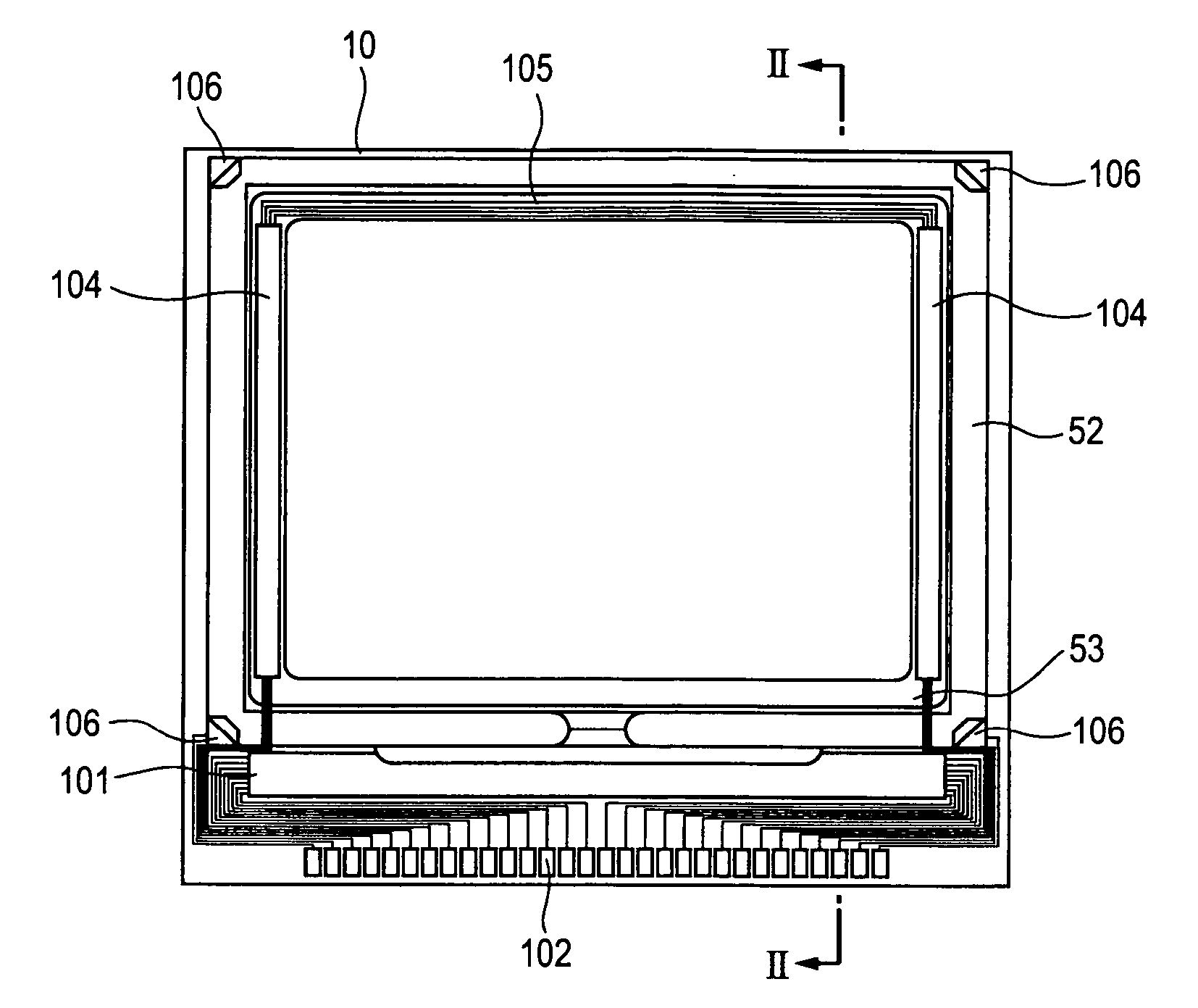
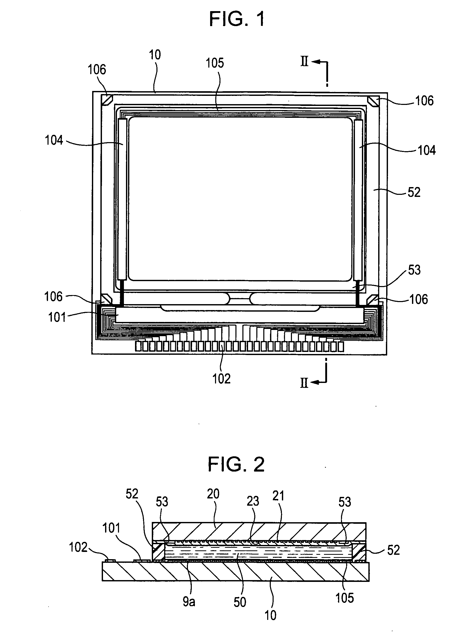
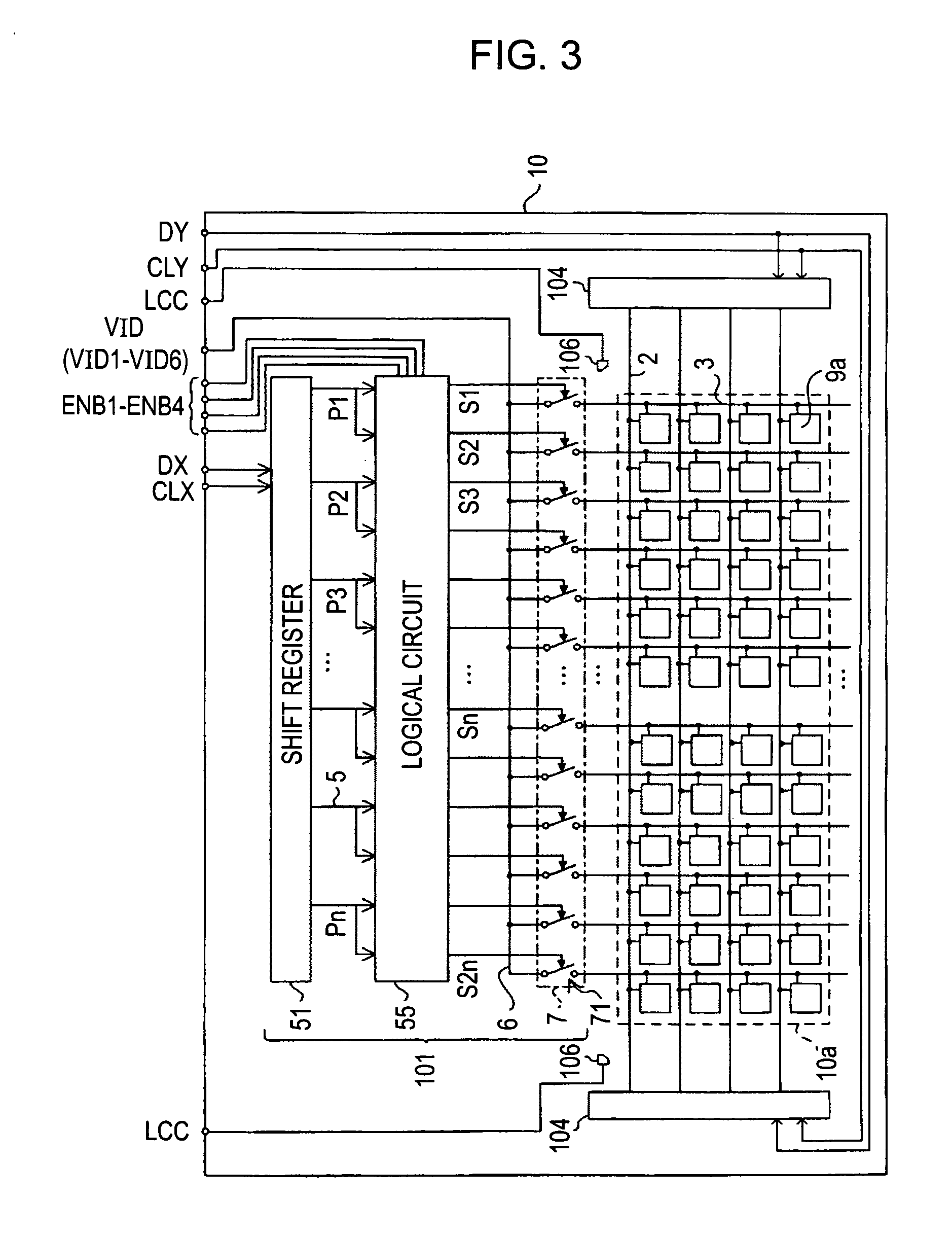
[0047] The overall structure of a liquid crystal display device according to an embodiment of the invention will be described with reference to FIGS. 1 to 3. FIG. 1 is a plan view of the liquid crystal display device, as viewed from a counter substrate, and FIG. 2 is a cross-sectional view taken along the line II-II of FIG. 1.

[0048] In FIGS. 1 and 2, the liquid crystal display device includes a TFT array substrate 10 and a counter substrate 20 which are opposite to each other. A liquid crystal layer 50 is interposed between the TFT array substrate 10 and the counter substrate 20, and the TFT array substrate 10 and the counter substrate 20 are bonded to each other by a sealing material 52 provided in a sealing region located aro...


PUM

PropertyMeasurementUnit
transmissionaaaaaaaaaa
widthaaaaaaaaaa
pulse widthsaaaaaaaaaa

Abstract

There is provided a circuit for driving an electro-optical device including a plurality of data lines, a plurality of scanning lines extending perpendicular to the plurality of data lines, and a plurality of pixel units that are electrically connected to the data lines and the scanning lines, respectively, and that are arranged in an image display region. The circuit for driving an electro-optical device includes a shift register that sequentially outputs transmission signals from each stage thereof; a plurality of branch wiring lines which are provided corresponding to the respective stages, and each of which has an input terminal to which the transmission signals are input and m output terminals, where m is a natural number equal to or greater than 2, which are branched from the input terminal and through which the input transmission signals are output; a plurality of enable signal supply lines that respectively supply m types of enable signals having different output timings and a predetermined pulse width smaller than that of the transmission signal; an enable circuit that outputs signals whose pulse widths are shaped to the predetermined pulse width, based on the enable signals; and a sampling circuit that samples image signals, based on the shaped signals, and then outputs them to the plurality of data lines, respectively. The enable circuit includes a plurality of unit circuits. The unit circuits electrically connect the m branched output terminals to the enable signal supply lines for supplying the different types of enable signals, respectively. Each group is composed of m unit circuits, and the unit circuits belonging to the group have the same layout.

Description

BACKGROUND OF THE INVENTION [0001] 1. Technical Field [0002] The present invention relates to an electro-optical-device driving circuit mounted in an electro-optical device, such as a liquid crystal display device, to an electro-optical device, and to an electronic apparatus including an electro-optical device. [0003] 2. Related Art [0004] This type of driving circuit is composed of, for example, a data line driving circuit for driving data lines and a scanning line driving circuit for driving scanning lines, which are provided on a substrate of an electro-optical device, such as a liquid crystal display device. The driving circuit samples image signals supplied to image signal lines at the pulse timing of a sampling-circuit driving signal and then outputs the sampled signals to the data lines. In particular, when a driving frequency is high, a front end and a rear end of the sampling-circuit driving signal, in terms of phase, which is used for sampling, hardly overlap each other in...

Claims


Application Information

Patent Timeline
Patent Type & Authority Applications(United States)
IPC IPC(8): G02F1/1343
CPCG09G3/3688G02F1/13454G02F1/133
Inventor MOCHIZUKI, HIROAKI
Owner SEIKO EPSON CORP
Why Eureka
Try Eureka