Surface emitting laser with an integrated absorber

a laser and absorber technology, applied in the field of lasers, can solve the problems of monolithic structures not being able to achieve the formation of a single short pulse circulating in the cavity, and achieve the effect of generating/distributing signals,

Inactive Publication Date: 2006-02-09
TAHOE RES LTD
View PDF17 Cites 50 Cited by
  • Summary
  • Abstract
  • Description
  • Claims
  • Application Information

AI Technical Summary

Problems solved by technology

After many round-trips, this often leads to the formation of a single short pulse c

Method used


Image

  • Surface emitting laser with an integrated absorber
  • Surface emitting laser with an integrated absorber
  • Surface emitting laser with an integrated absorber

Examples


Embodiment Construction

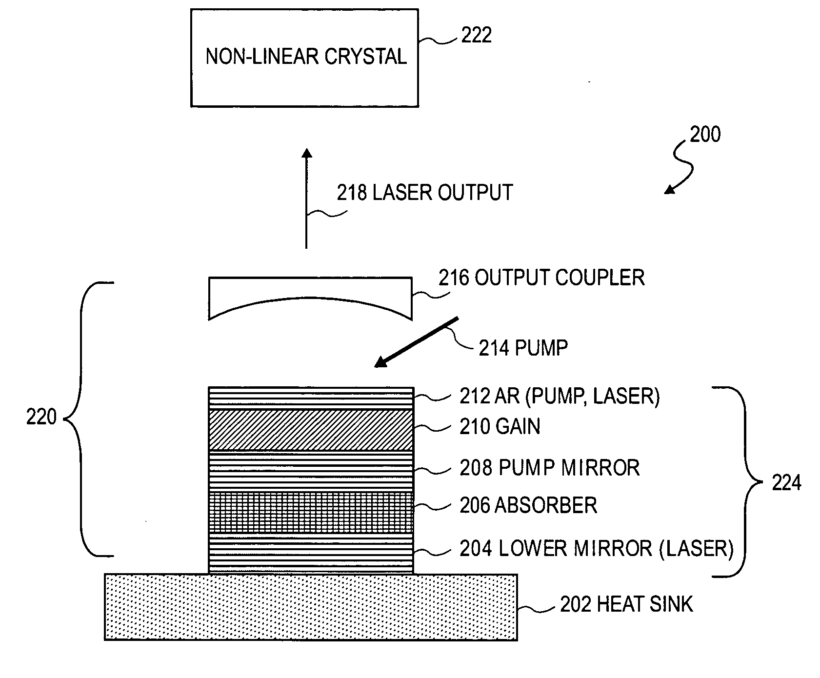
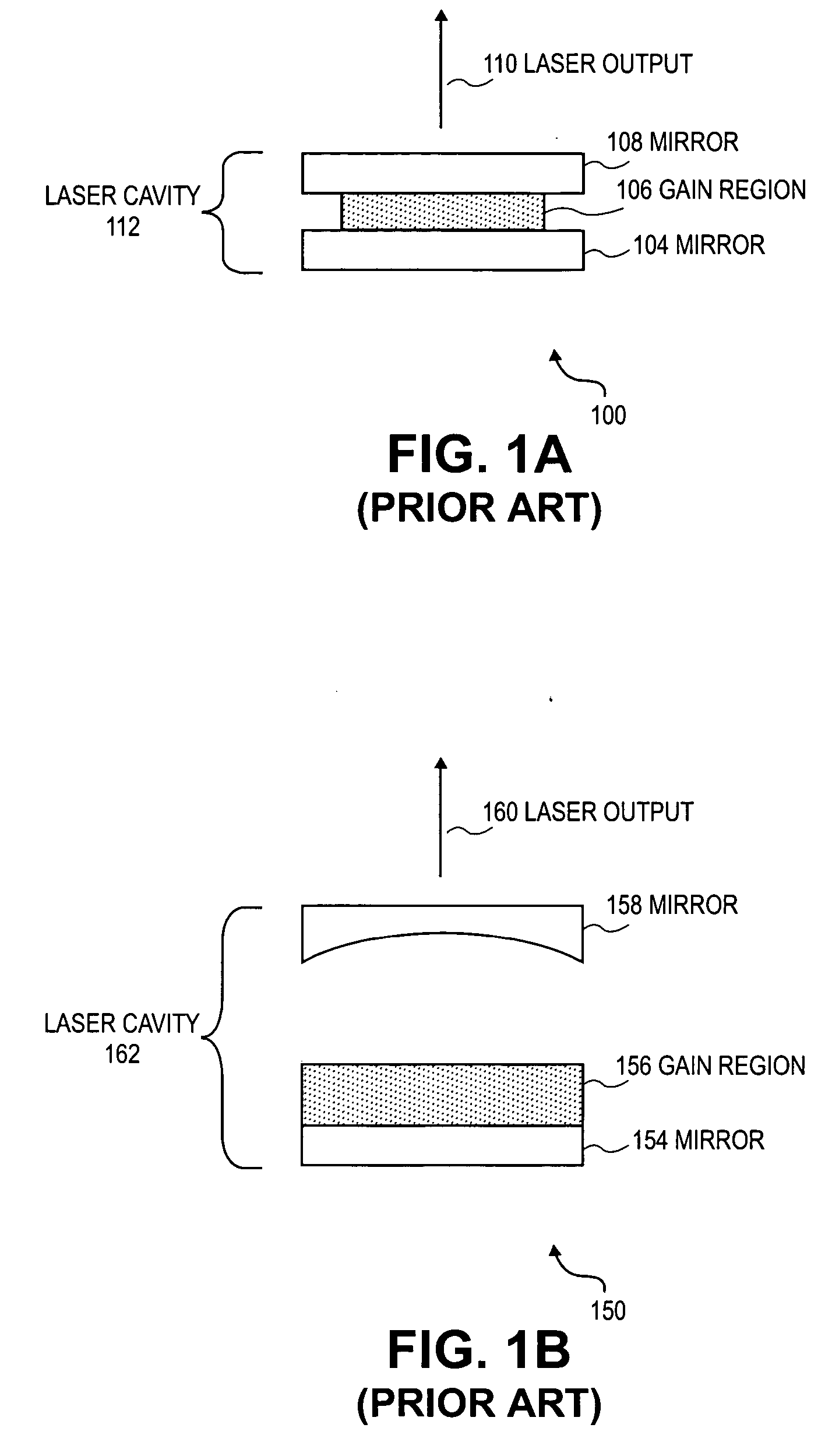
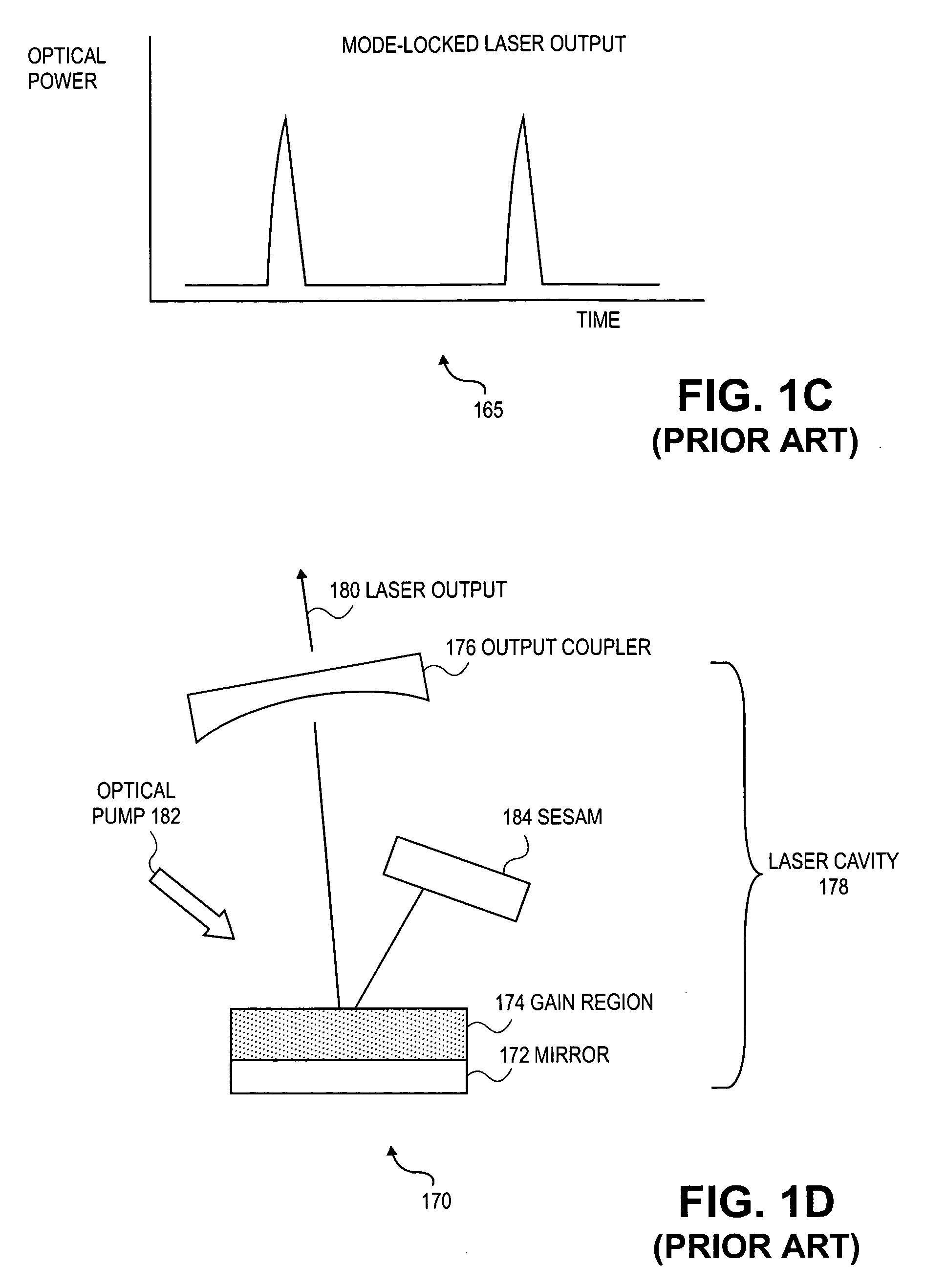
[0035] Embodiments of a surface emitting laser with an integrated absorber are described herein. In the following description, numerous specific details are set forth to provide a thorough understanding of embodiments of the invention. One skilled in the relevant art will recognize, however, that embodiments of the invention can be practiced without one or more of the specific details, or with other methods, components, materials, etc. In other instances, well-known structures, materials, or operations are not shown or described in detail to avoid obscuring aspects of the invention.

[0036] Reference throughout this specification to “one embodiment” or “an embodiment” means that a particular feature, structure, or characteristic described in connection with the embodiment is included in at least one embodiment of the present invention. Thus, the appearances of the phrases “in one embodiment” or “in an embodiment” in various places throughout this specification are not necessarily all...


PUM


Abstract

A surface emitting laser (SEL) with an integrated absorber. A lower mirror and an output coupler define a laser cavity of the SEL. A monolithic gain structure positioned in the laser cavity includes a gain region and an absorber, wherein a saturation fluence of the absorber is less than a saturation fluence of the gain region.

Description

BACKGROUND [0001] 1. Field of Invention [0002] The field of invention relates generally to lasers and, more specifically but not exclusively, relates to a surface emitting laser with an integrated absorber. [0003] 2. Background Information [0004] Semiconductor lasers have a variety of applications including communication systems and consumer electronics. Generally, semiconductor lasers may be categorized as edge-emitting lasers or surface emitting lasers (SELs). Edge-emitting lasers emit radiation parallel to the semiconductor wafer surface while SELs emit radiation perpendicular to the semiconductor wafer surface. Excitation of the gain region of semiconductor lasers may be through optical pumping or electrical pumping. [0005] Two common types of SELs are vertical cavity surface emitting laser (VCSEL) and vertical external cavity surface emitting laser (VECSEL). Referring to FIG. 1A, a VCSEL 100 is shown. A gain region 106 is sandwiched between mirror 104 and mirror 108. Such mirro...

Claims


Application Information

Patent Timeline
IPC IPC(8): H01S3/30G06F1/10H01S3/06H01S3/098H01S5/024H01S5/026H01S5/04H01S5/06H01S5/065H01S5/10H01S5/14H01S5/183H01S5/42
CPCG06F1/105H01S5/423H01S3/0604H01S3/0615H01S3/0627H01S3/094084H01S3/1115H01S3/1118H01S5/024H01S5/041H01S5/0609H01S5/0657H01S5/141H01S5/18302H01S5/18308H01S5/18341H01S5/18358H01S5/18388H01S3/0092
Inventor YOUNG, IAN A.KELLER, URSULAUNOLD, HEIKOPASCHOTTA, RUDIGERSCHON, SILKE
Owner TAHOE RES LTD
Why Eureka
Try Eureka