
Method and apparatus for thermal modeling and analysis of semiconductor chip designs

a technology of semiconductor chips and thermal modeling, applied in the field of semiconductor chip design, can solve the problems of not always conforming to design standards or parameters, consuming too many resources (e.g., processing or memory), and most known methods for modeling or simulating thermal gradients of semiconductor chips for analysis, etc., to be feasible applied to the modeling of full-chip thermal gradients

Active Publication Date: 2006-02-09
KEYSIGHT TECH
View PDF35 Cites 62 Cited by
  • Summary
  • Abstract
  • Description
  • Claims
  • Application Information

AI Technical Summary

Benefits of technology

The patent describes a method and device for analyzing the temperature of semiconductor chip designs. This is done by using a technique called geometric multi-grid, which calculates the temperature of the chip design based on its physical attributes. The technique helps identify areas of the chip that are hot or cold, which can help improve its performance and reliability.

Problems solved by technology

The resultant designs thus do not always conform to the design standards or parameters.
Moreover, most known methods for modeling or simulating thermal gradients of semiconductor chips for analysis are too generic, too computationally complex, or consume too many resources (e.g., processing or memory) to be feasibly applied to the modeling of full-chip thermal gradients.

Method used


Image

  • Method and apparatus for thermal modeling and analysis of semiconductor chip designs
  • Method and apparatus for thermal modeling and analysis of semiconductor chip designs
  • Method and apparatus for thermal modeling and analysis of semiconductor chip designs

Examples


Embodiment Construction

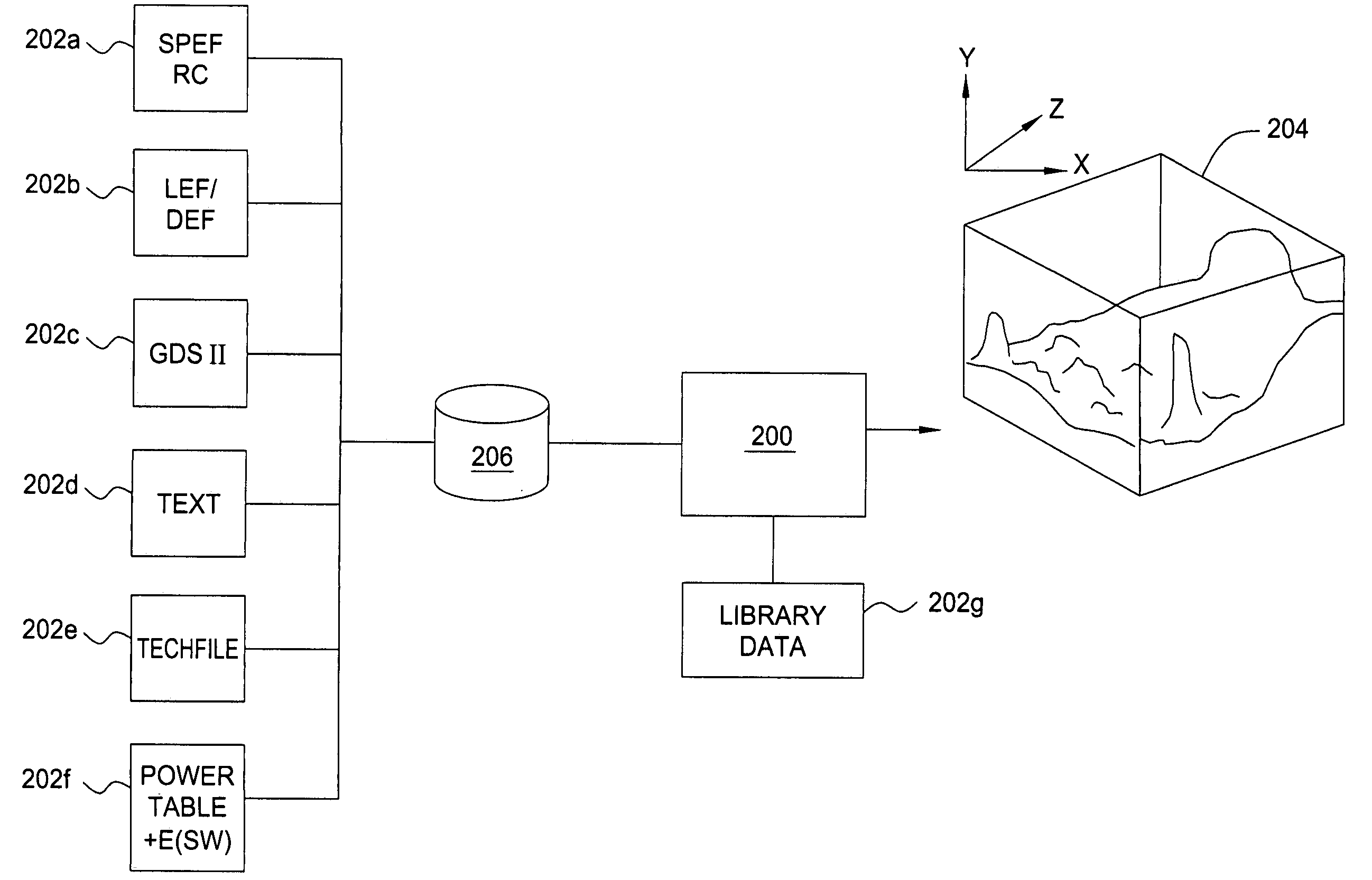
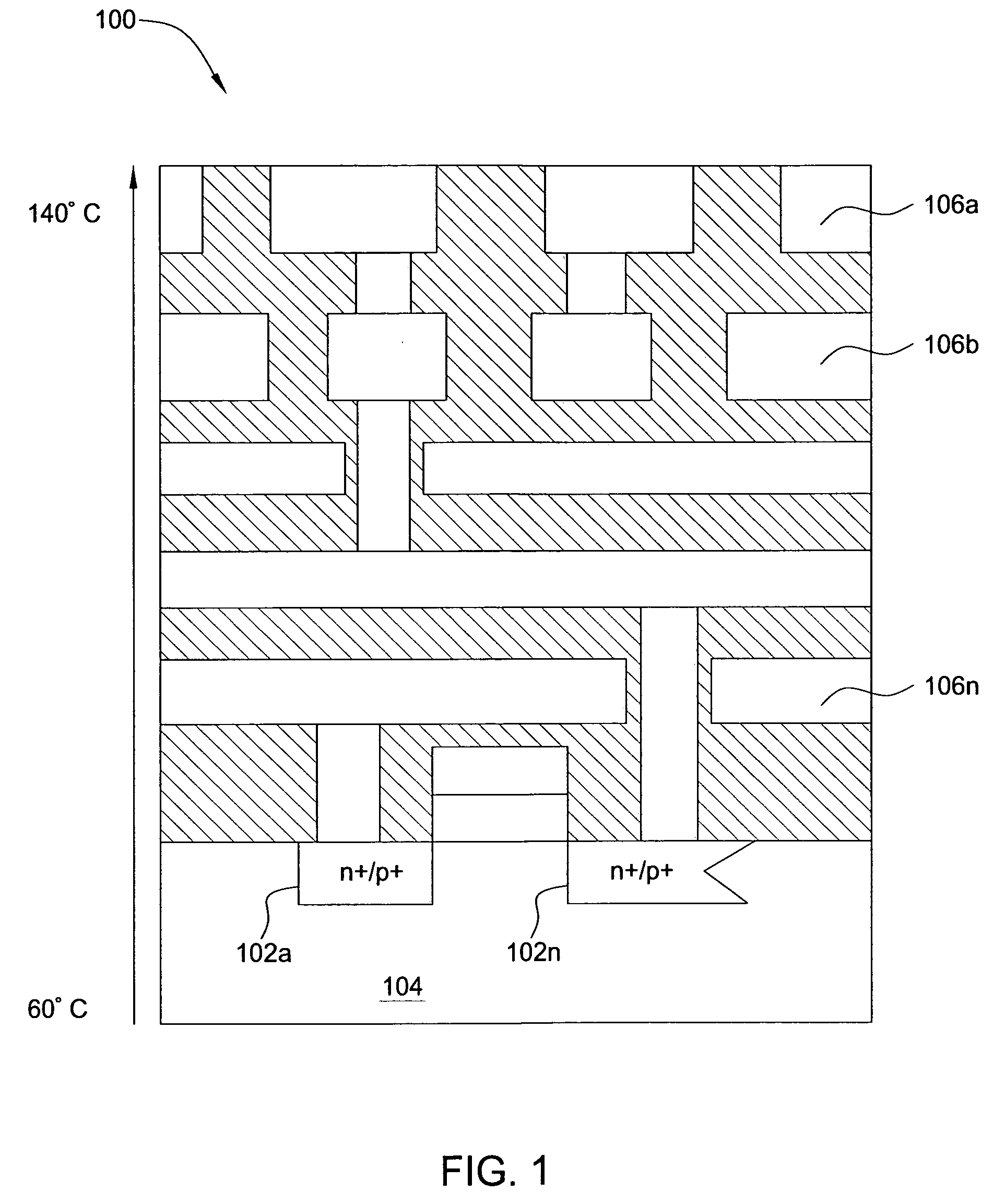
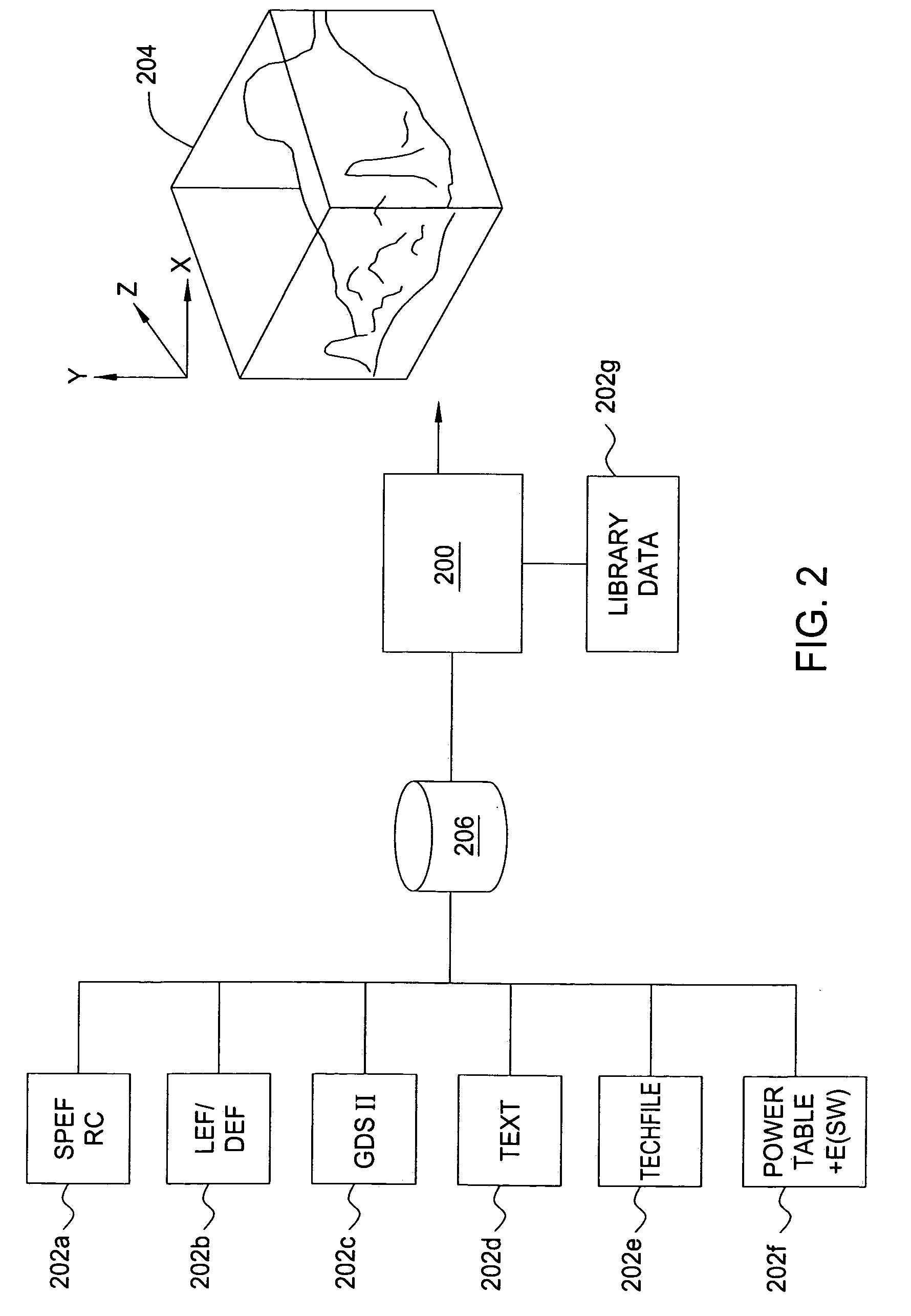
[0027] Embodiments of the invention generally provide a method and apparatus for thermal modeling and analysis of semiconductor chip designs. By providing temperature data that is computed or calculated based on actual chip information instead of estimated temperature data (e.g., based on an assumed uniform temperature), and modeling this temperature data in accordance with a tailored multi-grid technique, more accurate understanding of the thermal gradients produced by an operating semiconductor chip design can be attained. Moreover, the multi-grid technique described herein can be used to model the thermal gradient without building a problem matrix, and is thus quicker and less computationally intensive than existing modeling techniques using multi-grid solvers.

[0028] As used herein, the term “semiconductor chip” refers to any type of semiconductor chip, which might employ analog and / or digital design techniques and which might be fabricated in a variety of fabrication methodolog...


PUM


Abstract

A method and apparatus for modeling and thermal analysis of semiconductor chip designs is provided. One embodiment of a novel method for performing thermal testing of a semiconductor chip design includes calculating full-chip temperatures over the semiconductor chip design (e.g., to identify steep thermal gradients) and modeling the full-chip temperatures in accordance with a geometric multi-grid technique. The geometric multi-grid technique is tailored to determine temperatures within the semiconductor chip design based at least in part on the physical attributes or geometry of the design.

Description

CROSS-REFERENCE TO RELATED APPLICATIONS [0001] This application claims the benefit of U.S. Provisional Patent Application No. 60 / 587,313, filed Jul. 13, 2004 (entitled “Efficient Full-Chip Thermal Modeling and Analysis”), which is herein incorporated by reference in its entirety. In addition, this application is a continuation-in-part of U.S. patent application Ser. No. 11 / 039,737, filed Jan. 20, 2005 (entitled “Method and Apparatus For Retrofitting Semiconductor Chip Performance Analysis Tools With Full-Chip Thermal Analysis Capabilities”, hereinafter “the '737 application”), which is herein incorporated by reference in its entirety. In turn, the '737 application claims the benefit of U.S. Provisional Patent Application No. 60 / 599,098, filed Aug. 5, 2004 (entitled “Method And Apparatus For Retrofitting Commercial Timing, Delay, Voltage And Power Analysis Tools With Temperature Gradients”), which is herein incorporated by reference in its entirety. The '737 application is also a con...

Claims


Application Information

Patent Timeline
Patent Type & Authority Applications(United States)
IPC IPC(8): G06F17/50
CPCG06F17/5009G06F17/5018G06F17/5036G06F2217/84G06F2217/78G06F2217/80G06F17/5081G06F30/398G06F30/367G06F2119/12G06F2119/08G06F30/23G06F30/20G06F2119/06
Inventor LI, PENGPILEGGI, LARRYASHEGHI, MEHDICHANDRA, RAJIT
Owner KEYSIGHT TECH
Learn More