Radio frequency identification (RFID) tag and manufacturing method thereof

a technology of radio frequency identification and rfid tag, which is applied in the direction of burglar alarm mechanical actuation, burglar alarm by hand-portable object removal, instruments, etc., can solve the problem that the loop antenna cannot be used in small rfid tag

Active Publication Date: 2006-02-16
FUJITSU LTD
View PDF9 Cites 171 Cited by
  • Summary
  • Abstract
  • Description
  • Claims
  • Application Information

AI Technical Summary

Benefits of technology

[0013] It is an object of the present invention to solve at least the problems in the conventional technology.

Problems solved by technology

The wave-absorbing material poses a problem in the communication process since it absorbs the radio waves (for instance, radio waves in the ultra high frequency (UHF) band) that are required by the RFID tag for transmission and reception. FIG. 26 and FIG. 27 are drawings of conventional well-known means that enhance the gain of an antenna. FIG. 26 is a cross-sectional view of a conventional RFID tag in which a plane antenna is provided on the wave-absorbing material. FIG. 27 is a cross-sectional view of a conventional RFID tag in which a loop antenna is provided on the wave-absorbing material.
Therefore, the loop antenna can not be employed in small RFID tags.

Method used


Image

  • Radio frequency identification (RFID) tag and manufacturing method thereof
  • Radio frequency identification (RFID) tag and manufacturing method thereof
  • Radio frequency identification (RFID) tag and manufacturing method thereof

Examples


first embodiment

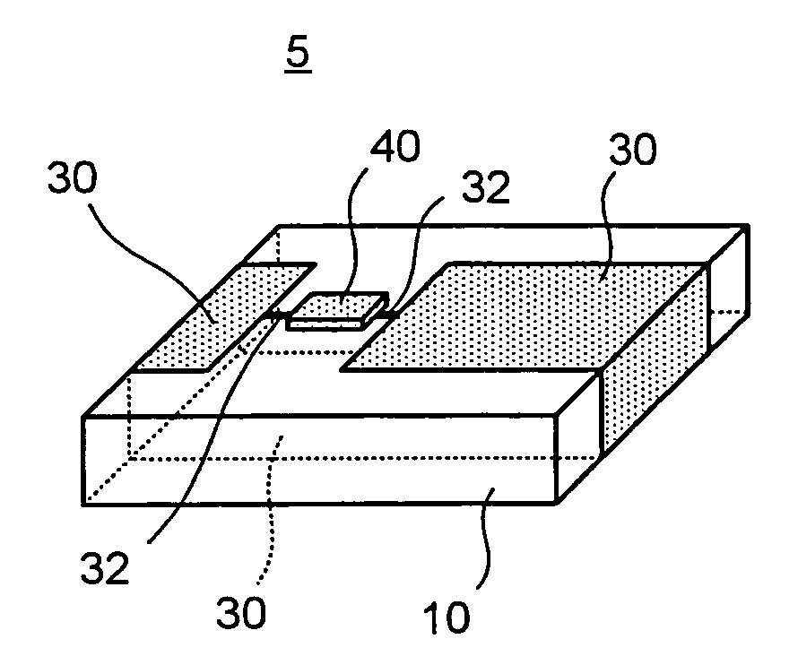
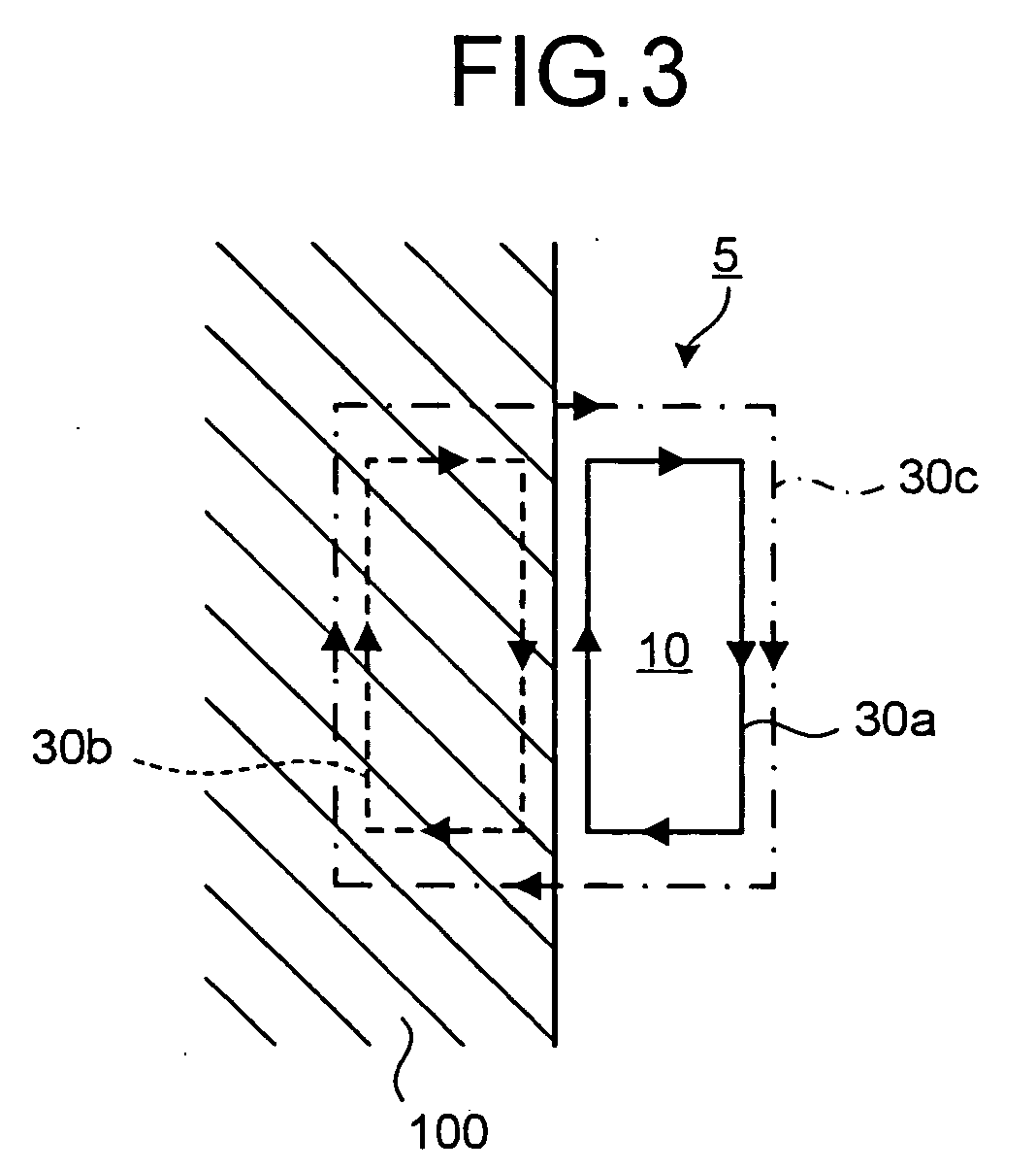
[0058] The RFID tag 5 that has a structure as described above that can transmit accurate radio wave information due to enhanced transmission gain of the antenna when receiving power supply and information from and transmitting the received information to an external device (not shown) contact-free. As a result, the reliability of the data communication can be increased. Though a rectangular dielectric member 10 has been used in the RFID tag 5 the dielectric member 10 may be of any shape (for instance, cylindrical, triangular prism, spherical, etc.) depending on the article it is intended for.

[0059]FIG. 4 is a perspective view of a RFID tag according to a second embodiment of the present invention. FIG. 5 is a top view of a film substrate. The parts in the second embodiment that are identical to those in the first embodiment are assigned the same reference numerals and their description is made very brief or skipped altogether.

second embodiment

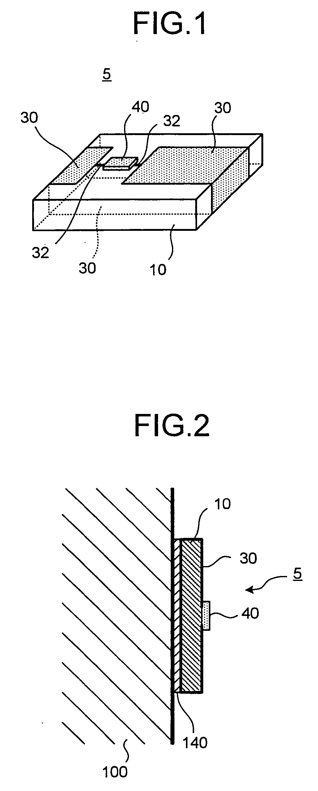
[0060] As shown in FIG. 4, the RFID tag 5 according to the present invention includes the dielectric member 10, a film substrate 20, and the IC chip 40. The film substrate 20 forms the antenna pattern 30 that transmits and receives data and is wrapped around the dielectric member 10. The IC chip 40 is connected to the antenna pattern 30.

[0061] The rectangular dielectric member 10 is composed of a dielectric material that has a designated dielectric constant and can be formed inexpensively using only glass-free resin. For instance, the dielectric member 10 can be formed with resin such as polytetrafluoroethylene (PTFE), polyphenylether (PPE), and the like, that have excellent processibility and mechanical properties.

[0062] As shown in FIG. 4 and FIG. 5, the antenna pattern 30 that forms the transceiving loop antenna is formed on the film substrate 20 by a printing means. The film substrate 20 is composed of a flexible thermoplastic material. Polyethylene terephthalate (hereinafter, ...

third embodiment

[0070]FIG. 9 is a perspective view of the RFID tag according to the present invention. FIG. 10 is a top view of the film substrate. As shown in FIG. 9 and FIG. 10, the chip pad 32 is provided parallel to the length of the antenna pattern 30 in such a way that the position of the feeding point of the IC chip 40 can be adjusted.

[0071] In other words, the chip pad 32 is connected to the antenna pattern 30 by a connector 32a and is provided parallel to the antenna pattern 30. The chip pad 32 and the connector 32a are composed of the same material as the antenna pattern 30 and are simultaneously formed when the antenna pattern 30 is printed on the film substrate 20.

[0072] As shown in FIG. 9, the film substrate 20 is wrapped around and secured to the dielectric member 10 in such a way that the antenna pattern 30 functions as a patch antenna. The IC chip 40 is mounted after the film substrate 20 is secured to the dielectric member 10 and the position of the feeding point is adjusted.

[007...


PUM

PropertyMeasurementUnit
dielectric constantaaaaaaaaaa
dielectric constantsaaaaaaaaaa
dielectric lossesaaaaaaaaaa

Abstract

An RFID tag includes a dielectric member, an antenna pattern formed on and around a surface of the dielectric member, and an IC chip that is electrically connected to the antenna pattern by means of two chip pads.

Description

BACKGROUND OF THE INVENTION [0001] 1) Field of the Invention [0002] The present invention relates to a radio frequency identification (RFID) tag such as a non-contact integrated circuit (IC) card, which receives power supply and information from, and transmits information to, an external device. The “RFID tag” used in the present invention is also known to one skilled in the art as an “RFID tag inlay”, inlay being an internal constituent part (inlay) used in the “RFID tag”. The “RFID tag” is also known as a “wireless IC tag”. [0003] 2) Description of the Related Art [0004] RFID tags such as a non-contact integrated circuit that receive using radio waves, power supply and information from an external device such as an IC card reader / writer and then transmit the received information to the external device contact-free are being used in recent years. A typical RFID tag includes an antenna pattern and an integrated circuit (IC) chip. The antenna pattern, which transmits and receives dat...

Claims


Application Information

Patent Timeline
Patent Type & Authority Applications(United States)
IPC IPC(8): G06K19/06G08B13/14
CPCG06K19/07749G06K19/07771H01L2224/16H01L2924/01078H01L2924/15165H01Q1/2208Y10T29/49117H01Q1/2225H01Q7/00H01Q23/00H01Q1/2216Y10T29/49124H01L2924/15153H01L2924/00011H01L2924/00014H01L2224/0401G06K19/07G06K19/077
Inventor BABA, SHUNJIMANIWA, TORUYAMAGAJO, TAKASHIKAI, MANABUHAYASHI, HIROYUKI
Owner FUJITSU LTD
Why Eureka
Try Eureka