
Wire-wound type chip coil and method of adjusting a characteristic thereof

a chip coil and wire-wound technology, applied in the direction of transformer/inductance coil/winding/connection, inductance with magnetic core, etc., can solve the problems of difficult process needed to adjust the matching between a circuit element and a transmission line, and limit the inductance to corresponding values. , to achieve the effect of simple structur

Inactive Publication Date: 2006-02-16
MURATA MFG CO LTD
View PDF6 Cites 8 Cited by
  • Summary
  • Abstract
  • Description
  • Claims
  • Application Information

AI Technical Summary

Benefits of technology

This approach enables the achievement of a greater number of different inductance values, reduces coil resistance, and enhances the Q value, thereby minimizing loss in matching circuits and allowing for precise adjustments within the same size constraints.

Problems solved by technology

In recent high-frequency circuits, a very difficult process is needed to adjust the matching between a circuit element and a transmission line.
However, in conventional wire-wound type chip coils having a structure such as that described above, only integers are allowed for the number of turns of a winding connected between electrodes, and inductance is limited to corresponding values.

Method used


Image

  • Wire-wound type chip coil and method of adjusting a characteristic thereof
  • Wire-wound type chip coil and method of adjusting a characteristic thereof
  • Wire-wound type chip coil and method of adjusting a characteristic thereof

Examples


first embodiment

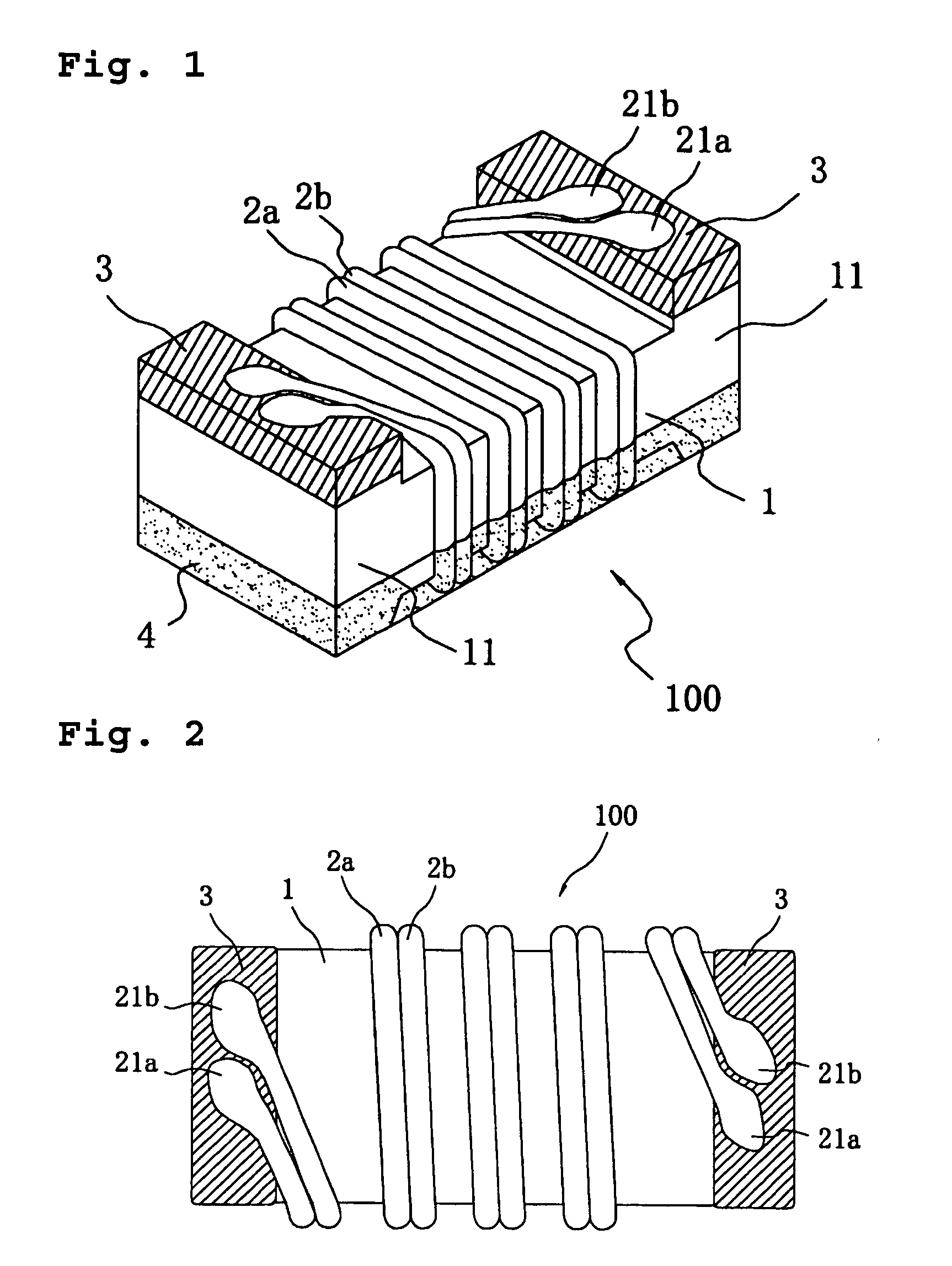
[0052] In the table shown in FIG. 11, values of inductance obtained by winding two conductive wires with a diameter of about 50 μm regularly in a single layer around a 1005-size core are shown in a row denoted by “FIRST EMBODIMENT”. In this case, in contrast to the “CONVENTIONAL TECHNIQUE” in which 1.5 nH and 2.7 nH are obtained respectively for one-turn and two-turn coils of one conductive wire, use of two conductive wires results in reductions in inductance down to about 1.2 nH and about 2.4 nH for one-turn and two-turn coils respectively.

[0053] As described earlier, when a single conductive wire with a diameter of about 80 μm is wound one turn around a 1608-size core, resultant inductance is about 2.2 nH. Herein, if the single conductive wire is replaced with two conductive wires, the inductance decreases to about 1.8 nH. If the number of substantially parallel conductive wires is further increased, a further reduction in inductance is achieved. Thus, by properly selecting the nu...

second embodiment

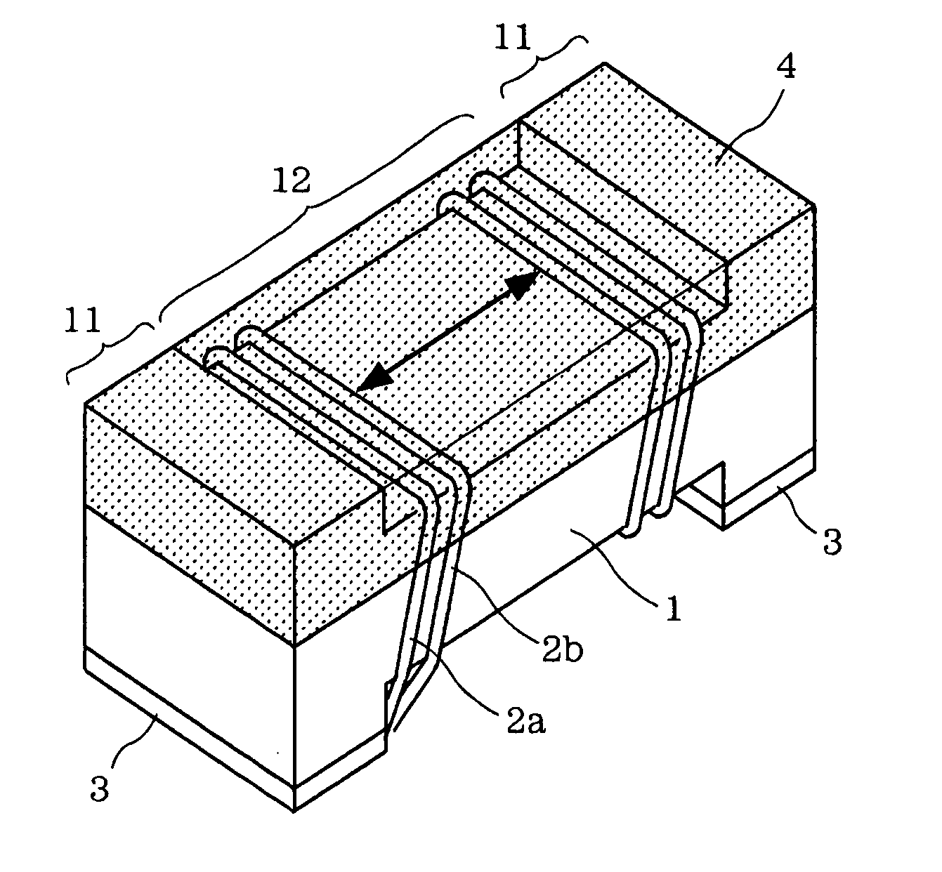
[0058] In this wire-wound type chip coil according to the second preferred embodiment, the conductive wires 2a and 2b are wound around the main portion 12 of the core 1 such that the conductive wires 2a and 2b are spaced from each other and such that the distance between any adjacent wires becomes substantially equal. In the table shown in FIG. 11, in a row denoted by “SECOND EMBODIMENT”, shown are values of inductance obtained by winding two conductive wires with a diameter of about 50 μm around a 1005-size core such that the conductive wires are spaced from each other and such that the distance between any adjacent wires becomes substantially equal. As can be seen, an inductance of about 1.1 nH to about 1.3 nH is obtained by a one-turn coil of two wires, and inductance of about 1.8 nH to about 2.4 nH is obtained by a two-turn coil.

[0059] Thus, inductance of about 2.4 nH for a two-turn regularly-wound single-layer coil can be reduced to about 1.8 nH by expanding the space between t...

third embodiment

[0063] In this preferred embodiment, unlike the wire-wound type chip coil according to the second preferred embodiment, two conductive wires 2a and 2b are regularly wound in a single layer around the main portion 12 of the core, and the space between one of the two conductive wires at a certain turn and the other one of the two conductive wires at an adjacent turn is adjusted so as to obtain a desired value of inductance. In the table shown in FIG. 11, in a row denoted by “THIRD EMBODIMENT”, shown are values of inductance obtained by winding two conductive wires with a diameter of about 50 μm around a 1005-size core. As can be seen, inductance of about 2.0 nH to about 2.4 nH is obtained by a by a two-turn coil of two wires.

[0064]FIG. 9 shows the inductance as a function of the space between the two conductive wires, for a two-turn coil using conductive wires with a diameter of about 50 μm. Inductance of about 2.2 nH is obtained when the wire-to-wire space between adjacent turns is a...


PUM

PropertyMeasurementUnit
thicknessaaaaaaaaaa
diametersaaaaaaaaaa
inductanceaaaaaaaaaa

Abstract

A wire-wound type chip coil can take various inductance values while maintaining its outer dimension at a specific fixed value. A chip coil is formed by winding at least two conductive wires regularly in a single layer around a core made of a magnetic material and firmly connecting both ends of each conductive wire to terminal electrodes disposed on respective flanges of the core. This makes it possible to obtain a great current capacity. Furthermore, the inductance decreases because of an increase in the magnetic path length. A great number of different inductance values can be easily obtained by properly selecting parameters including the number of substantially parallel conductive wires, the diameter of each conductive wire, and the number of turns.

Description

[0001] This application is a Divisional Application of U.S. patent application Ser. No. 10 / 215,083 filed Aug. 9, 2002, currently pending.BACKGROUND OF THE INVENTION [0002] 1. Field of the Invention [0003] The present invention relates to a wire-wound type chip coil and in particular, a small-sized wire-wound type chip coil for use, for example, in a high-frequency circuit, and also to a method of adjusting a characteristic of a wire-wound type chip coil. [0004] 2. Description of the Related Art [0005] The structure of a conventional wire-wound type chip coil is described below with reference to FIG. 12. [0006]FIG. 12 is a perspective view illustrating the external appearance of a wire-wound type chip coil according to a conventional technique. [0007] In FIG. 12, reference numeral 100 denotes a chip coil, 1 denotes a core, 11 denotes flanges, 2 denotes a conductive wire, 21 denotes end portions of the conductive wire, 3 denotes terminal electrodes, and 4 denotes a coating resin. [000...

Claims


Application Information

Patent Timeline
Patent Type & Authority Applications(United States)
IPC IPC(8): H01F5/00H01F41/00H01F17/04H01F27/29
CPCH01F17/045H01F27/292Y10T29/49073Y10T29/49076Y10T29/49071Y10T29/4902
Inventor HIRAI, SHINYATOI, TAKAOMITSUBANA, KATSUHIKOYASUZAWA, HIROYUKI
Owner MURATA MFG CO LTD
Learn More