Method for the surface activation on the metalization of electronic devices

Inactive Publication Date: 2006-02-23
NATIONAL TSING HUA UNIVERSITY
View PDF1 Cites 4 Cited by
  • Summary
  • Abstract
  • Description
  • Claims
  • Application Information

AI Technical Summary

Benefits of technology

[0014] Accordingly, electroless Cu plating in the deep 100 nm scaled line-width ULSI interconnect metallization has been successfully achieved by the Pd plasma implantation catalytic treatment. This results in an extraordinary ability for filling the 100 nm line-width vias and trenches for gaining high quality electroless plated Cu interconnect, and thus qualifies to substitute for the traditional wet activation by SnCl2 and PdCl2 soluti

Problems solved by technology

The interconnect manufactured with the conventional physical vapor phase deposition method is no longer suitable due to the problems caused by deep trench or high aspect ration via.
The discontinuity in the copper seed layer may cause the non-uniform distribution of the electroplating current and eventually lead to the formation of micro voids in the trench and the vias.
The formation of micro voids not only increases the resistance of the interconnect, but also affects the device reliability.
The composition of the copper solution was difficult to control and prone to decomposition in the 1950s.
Unfortunately, the seed layer of this type cannot provide sufficient adhesion as the deposit

Method used


Image

  • Method for the surface activation on the metalization of electronic devices
  • Method for the surface activation on the metalization of electronic devices
  • Method for the surface activation on the metalization of electronic devices

Examples


Example

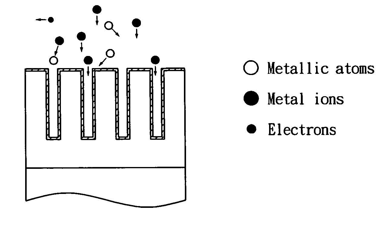
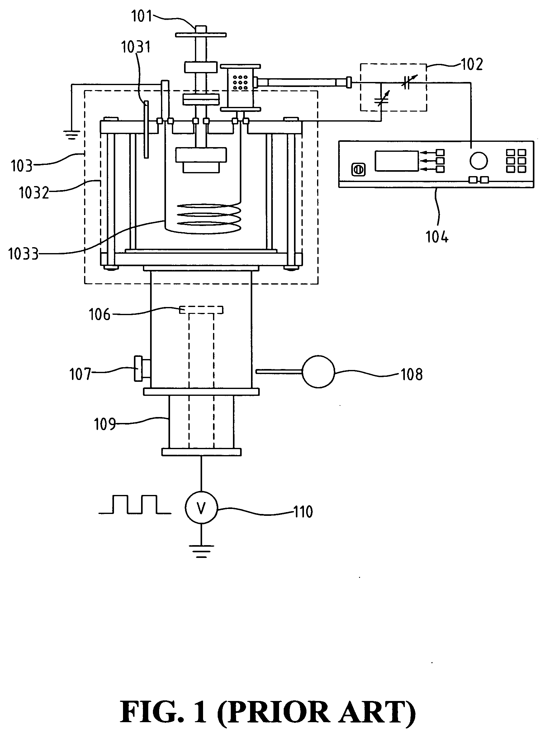
[0023]FIG. 1 shows a schematic view of a plasma-immersion ion implantation system using an ionized sputter. Referring to FIG. 1, the plasma-immersion ion implantation system includes a sputtering gun 101, a matching box 102, a vacuum chamber 103 coupled with sputtering gun 101, further including a gas-in vent 1031, a RF shielding unit 1032 and a magnetic coil 1033 coupled with matching box 102, a RF power supply 104 coupled with matching box 102 to provide RF power to magnetic coil 1033, a wafer holder 106 for holding the wafer, a pumping 107, a vacuum gauge 108, a high voltage stage 109, and a negative pulsed bias 110 connected to high voltage stage 109. The Pd ions are sputtered from sputtering gun 101 at the top of vacuum chamber 103 and passing through magnetic coil 1033. Because the initial sputtered Pd plasma has a low ion density, the Pd atoms are ionized when passing through magnetic coil 1033. The ionized atoms are dragged by high voltage stage 109 connected to negative pul...


PUM

PropertyMeasurementUnit
Electric potential / voltageaaaaaaaaaa
Nanoscale particle sizeaaaaaaaaaa

Abstract

A method for surface activation on the metallization of electronic devices is provided. It uses plasma-immersion ion implantation and electroless plating to implant the seeds onto the diffusion barrier layer as catalyst for the electroless Cu plating to accomplish the ULSI interconnect metallization. It achieves electroless Cu plating in the deep 100 nm scaled line-width ULSI interconnect metallization by the Pd plasma implantation catalytic treatment. The method can fill the 100 nm line-width vias and trenches for gaining high quality electroless plated metal interconnects, and substitute for the traditional wet activation by SnCl2 and PdCl2 solution. For the plasma implanted seeds and electroless copper techniques, good Cu step coverage and gap-filling capability are observed in the trench and via metallization process with high adhesive strength. After thermal treatment, no obvious interfacial diffusion induced electric failure is found in the interface of the Cu/(implanted Pd)/TaN/FSG assembly. Good electric and interfacial structure reliability are observed in the process, too.

Description

FIELD OF THE INVENTION [0001] The present invention generally relates to a method for surface activation on the metallization of electronic devices, and more specifically to a plasma ion implantation method to form an active layer on electronic devices. BACKGROUND OF THE INVENTION [0002] The Damascene metallization technique, also called Damascene process, was proposed by IBM in 1983. The Damascene process differs from conventional metallization process in that the Damascene process first forms a pattern in the dielectric layer and then fills the gap (pattern) with metal, while the conventional aluminum process first forms a pattern using the metal before filling the dielectric layer. After the metallization, the Chemical Mechanic Polishing (CMP) method is used to flatten the surface and leave the metal in the trenches and vias. A multilevel interconnection device can be obtained by iterating the process for a few times. A diffusion barrier must be added between the copper and the d...

Claims


Application Information

Patent Timeline
IPC IPC(8): C23C14/00H01L21/4763
CPCC23C14/046C23C14/48H01L21/76859C23C18/38H01L21/76874H01J37/32412C23C18/1879H01L21/76864
Inventor SHIH, HAN-CHANGLIN, JIAN-HONGHSIEH, WEI-JENTSAI, YI-YINGCHEN, UEI-SHIN
Owner NATIONAL TSING HUA UNIVERSITY
Why Eureka
Try Eureka