Semiconductor device and manufacturing method of the same

A manufacturing method and semiconductor technology, applied in the fields of semiconductor/solid-state device manufacturing, semiconductor devices, semiconductor/solid-state device components, etc., can solve the problems of decreased electrical bonding area, disconnection, and increased connection resistance.

Active Publication Date: 2008-08-13
SANYO ELECTRIC CO LTD +1
View PDF4 Cites 0 Cited by
  • Summary
  • Abstract
  • Description
  • Claims
  • Application Information

AI Technical Summary

Problems solved by technology

Then, the electrical bonding area between the bump electrodes 52 and the penetration electrodes 62 decreases, so that the connection resistance increases or disconnection occurs, and the electrical connection characteristics may deteriorate.

Method used


Image

  • Semiconductor device and manufacturing method of the same
  • Semiconductor device and manufacturing method of the same
  • Semiconductor device and manufacturing method of the same

Examples


no. 1 approach

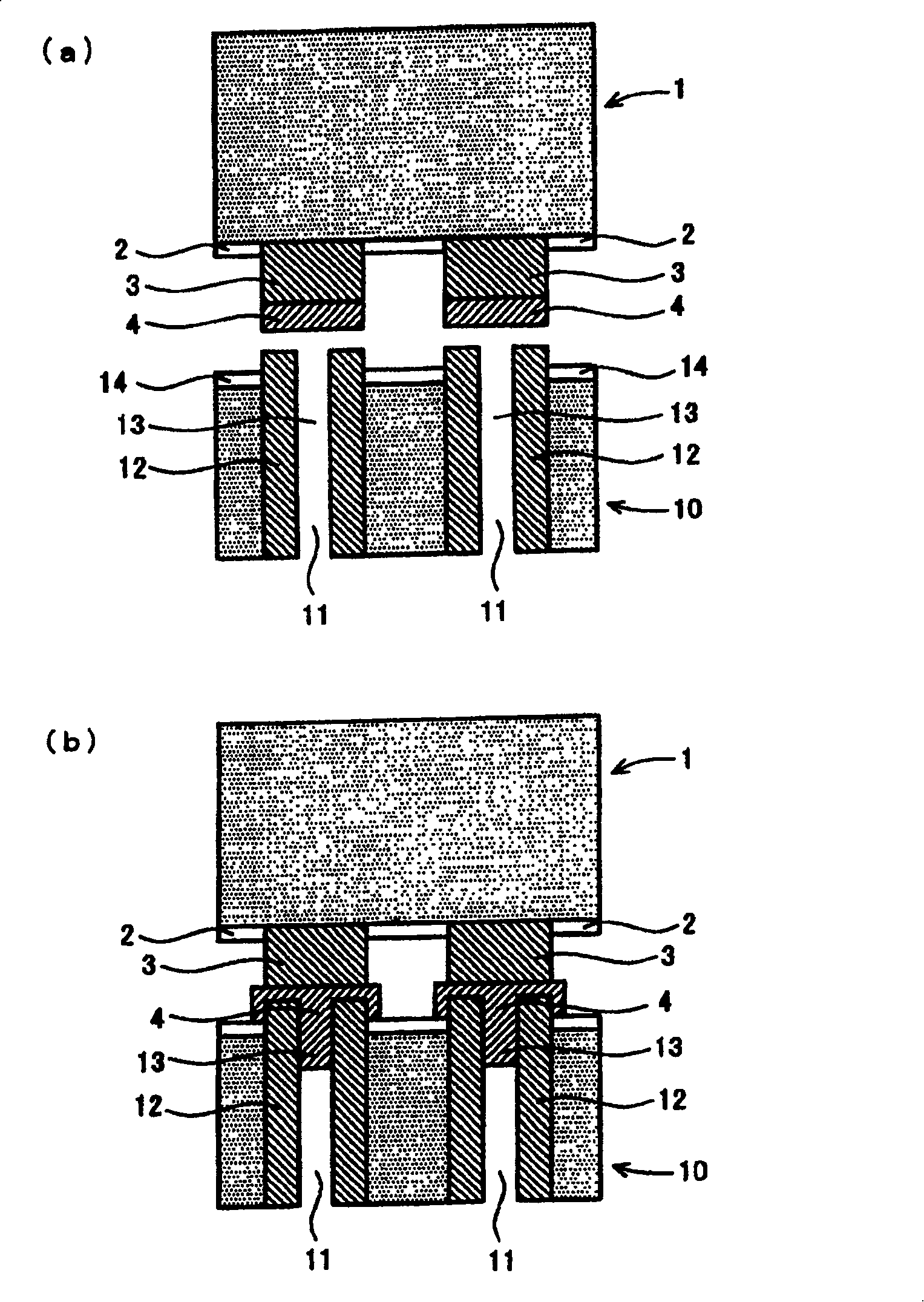
[0027] Such as figure 1 As shown in (a), a semiconductor integrated circuit (not shown) is formed on the surface of the first semiconductor chip 1, and a passivation film 2 made of a silicon nitride film (SiN film) is formed in order to protect the semiconductor integrated circuit. Then, a plurality of bump electrodes 3 are formed on the surface of the first semiconductor chip 1 as terminals for external connection of the semiconductor integrated circuit, and a low-melting point metal member 4 as an electrode connection member is attached to the front end thereof.

[0028] The plurality of bump electrodes 3 are made of metal such as copper, and can be formed using an electrolytic plating method. Its thickness is about 10 μm, and it is arranged at a fine pitch of about 20 μm or less. The low-melting-point metal member 4 is made of a metal different from the metal constituting the bump electrode 3 or the penetration electrode 12 described later, and is made of a different meta...


PUM

PropertyMeasurementUnit
thicknessaaaaaaaaaa

Abstract

This invention provides a semiconductor device which assures an accurate electric and medicinal connections between electrodes by connecting the plurality of semiconductor chips having electrodes with a low melting point metallic member. Bump electrodes are formed on a surface of a first semiconductor chip (1). Through holes (11) are formed in a second semiconductor chip (10). Through electrodes (12) having a clearance (13) in a central part of the through hole (11) are formed. A low melting point metallic member (4) is interposed between connection surfaces of the bump electrodes (3) and the through electrodes (12). A part of the low melting point metallic member, when melted is allowed to flow into the clearance (13). By this arrangement a short circuit between the bump electrodes (3, 3) caused by providing an excess amount of the low melting point member (4) in the space between adjacent bump electrodes (3, 3) can be prevented.

Description

technical field [0001] The present invention relates to a manufacturing method of a semiconductor device, in particular to a mounting technology of a semiconductor device having a through-electrode. Background technique [0002] Conventionally, there has been known a mounting structure in which a plurality of semiconductor chips having bump electrodes or penetrating electrodes are electrically and mechanically connected to each other via low-melting-point metal members such as solder. [0003] Figure 8 It is a sectional view explaining the manufacturing method of the semiconductor device of a conventional example. Such as Figure 8 As shown in (a), a passivation film 51 is formed on the surface of the first semiconductor chip 50 . Then, a plurality of bump electrodes 52 are formed on the surface of the first semiconductor chip 50, and a low melting point metal member 53 is attached on the front end thereof. [0004] On the other hand, in the second semiconductor chip 60 ,...

Claims


Application Information

Patent Timeline
Patent Type & Authority Patents(China)
IPC IPC(8): H01L21/60H01L23/48H01L23/28H01L25/18H01L21/52H01L25/065H01L25/07
CPCH01L2225/06513H01L2225/06541H01L25/0657H01L2924/01078H01L2924/01004H01L23/481H01L2225/06582H01L2224/16H01L21/52H01L21/60
Inventor 梅本光雄谷田一真
Owner SANYO ELECTRIC CO LTD
Why Eureka
Try Eureka