Semiconductor device and method for fabricating the same

a semiconductor device and semiconductor technology, applied in the field of semiconductor devices, can solve the problems of deterioration of the operation characteristics limit on the increase of the density of the field channel stop ions, and reduce the efficiency of the semiconductor device, so as to avoid the increase of the threshold voltage of the mos transistor, improve the isolation characteristics, and avoid the effect of junction diode characteristics

Inactive Publication Date: 2006-02-23
DONGBU ELECTRONICS CO LTD
View PDF5 Cites 18 Cited by
  • Summary
  • Abstract
  • Description
  • Claims
  • Application Information

AI Technical Summary

Benefits of technology

[0015] An object of the present invention is to provide a semiconductor device and a method for fabricating the same, to improve the isolation characteristics, avoid deterioration of the junction diode characteristics, and / or avoid the increase of a threshold voltage of the MOS transistor.

Problems solved by technology

However, in the method for fabricating the semiconductor device according to the related art, the wells and regions are divided primarily by the STI layers 14, which may cause a deterioration in the isolation characteristics.
As a result, the operation characteristics of the semiconductor device may deteriorate due to the leakage current.
Thus, as a threshold voltage Vth of MOS transistor is rising, it may cause a limit on the increase of the density of the field channel stop ions.

Method used


Image

  • Semiconductor device and method for fabricating the same
  • Semiconductor device and method for fabricating the same
  • Semiconductor device and method for fabricating the same

Examples


Embodiment Construction

[0026] Reference will now be made in detail to the preferred embodiments of the present invention, examples of which are illustrated in the accompanying drawings. Wherever possible, the same reference numbers will be used throughout the drawings to refer to the same or like parts.

[0027] Hereinafter, a semiconductor device and a method for fabricating the same according to the present invention will be described with reference to the accompanying drawings.

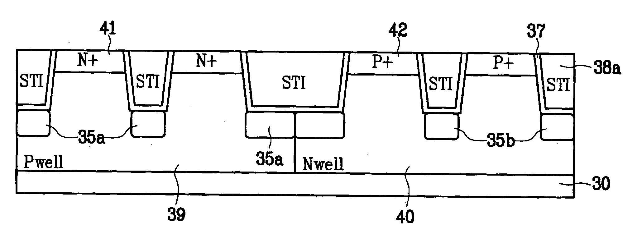
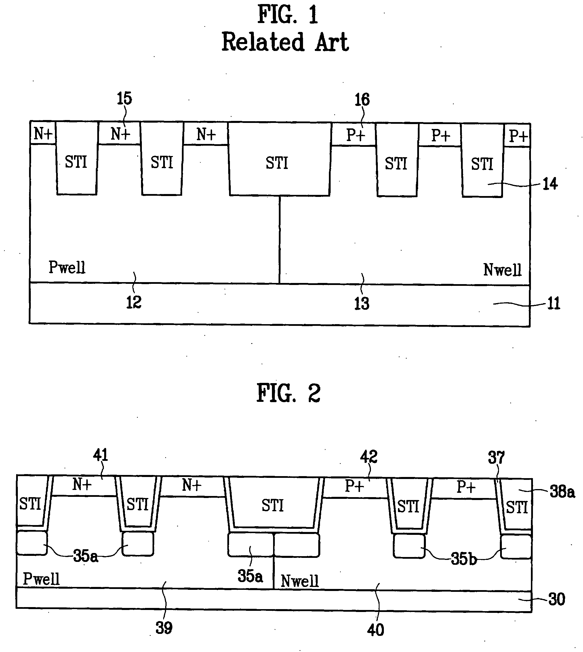
[0028]FIG. 2 is a cross sectional view of a semiconductor device according to the present invention.

[0029] As shown in FIG. 2, the semiconductor device according to the present invention includes a p-type well 39, an n-type well 40, an STI (Shallow Trench Isolation) layer 38a, a first field channel stop ion implantation layer 35a, a second field channel stop ion implantation layer 35b, a heavily-doped n-type impurity ion layer 41, and a heavily-doped n-type impurity ion layer 42.

[0030] At this time, the p-type well 39 and the n-...


PUM


Abstract

A semiconductor device and a method for fabricating the same may improve the isolation characteristics without deterioration of the junction diode characteristics and an increase in a threshold voltage of a MOS transistor. The device includes a semiconductor substrate; an STI layer in a predetermined portion of the semiconductor substrate, dividing the semiconductor substrate into an active region and a field region; and a field channel stop ion implantation layer in the semiconductor substrate under the STI layer.

Description

CROSS-REFERENCE TO RELATED APPLICATIONS [0001] This application claims the benefit of Korean Application No. P2004-66290 filed on Aug. 23, 2004, which is hereby incorporated by reference as if fully set forth herein. BACKGROUND OF THE INVENTION [0002] 1. Field of the Invention [0003] The present invention relates to a semiconductor device, and more particularly, to a semiconductor device having improved isolation structures and / or characteristics, and a method for fabricating the same. [0004] 2. Discussion of the Related Art [0005] Generally, a semiconductor device comprises a plurality of electrical devices, such as transistors, diodes and capacitors, on a semiconductor substrate. In this case, it is necessary for the semiconductor device to have an electrical device isolation layer. With high integration in the semiconductor device, the size of the electrical devices is scaled below a nano degree. Thus, the device isolation layer should have high isolation characteristics. [0006] ...

Claims


Application Information

Patent Timeline
Patent Type & Authority Applications(United States)
IPC IPC(8): H01L21/76
CPCH01L21/76229H01L21/823878H01L21/76237H01L21/76
Inventor JUNG, JIN HYO
Owner DONGBU ELECTRONICS CO LTD
Why Eureka
Try Eureka