Spin transistor using spin-filter effect and nonvolatile memory using spin transistor

a technology of filter effect and spin transistor, applied in the field of transistors, can solve the problems of low tmr ratio, low efficiency, nonvolatile, etc., and achieve the effect of increasing the operating speed and being difficult to avoid

Inactive Publication Date: 2006-03-02
JAPAN SCI & TECH CORP
View PDF11 Cites 17 Cited by
  • Summary
  • Abstract
  • Description
  • Claims
  • Application Information

AI Technical Summary

Benefits of technology

[0137] As described above, the spin-filter transistor and various spin transistors according to the various embodiments of the present embodiment are characterized in that the output characteristics can be controlled by the relative magnetization configuration of the pin layer and free layer within the device. The relative magnetization configuration is nonvolatile, namely, the device does not require the feeding of power for retaining the magnetization configuration. Thus, the device can store binary information in terms of the relative magnetization configuration in a nonvolatile fashion. Further, using the aforementioned output characteristics, the relative magnetization configuration can be electrically detected. Thus, a 1-bit nonvolatile memory cell can be configured with a single spin transistor. Using a nonvolatile memory circuit comprising a spin transistor according to the embodiments of the invention, the ratio of output signals as well as their magnitudes with respect to the stored information can be freely designed.
[0138] Thus, using the spin transistor according to the embodiments of the invention and a memory circuit comprising the spin transistor, the operating speed and the level of integration of a nonvolatile memory circuit can be increased.
[0139] While the present invention has been described with reference to various embodiments thereof, the present invention is not limited by any of these embodiments. It should be obvious to those skilled in the art that various modifications, improvements or combinations can be made.
[0140] In accordance with the spin-filter transistor of the present invention, the output characteristics can be greatly changed by the relative magnetization configuration of the ferromagnetic barrier layers.
[0141] A nonvolatile memory circuit comprising a memory cell employing this spin-filter transistor or a spin transistor with equivalent characteristics can store binary information in terms of the relative magnetization configuration of ferromagnets contained in the transistor. The relative magnetization configuration can also be detected electrically. Furthermore, using the nonvolatile memory circuit of the present invention, the output signals with respect to the stored information can be freely designed. Using such a spin transistor, a high-speed and high integration-density nonvolatile memory circuit can be realized that comprises a 1-bit nonvolatile memory cell made up of a single transistor.

Problems solved by technology

Because the MRAMs based on MTJ employ ferromagnets, they are nonvolatile, energy-saving, and fast.
However, before the MRAM can be realized as a next-generation nonvolatile memory, the following problems must be overcome.
However, since the TMR ratio also depends on the insulating film thickness, optimization of the tunnel resistance is limited.
However, the MTJ has the fundamental problem that, as the voltage drop across the ferromagnetic electrodes increases, the TMR ratio drops.
This phenomenon is inherently based on the TMR effect and hard to avoid as long as the configuration of magnetization is sensed based solely on the TMR effect.

Method used


Image

  • Spin transistor using spin-filter effect and nonvolatile memory using spin transistor
  • Spin transistor using spin-filter effect and nonvolatile memory using spin transistor
  • Spin transistor using spin-filter effect and nonvolatile memory using spin transistor

Examples


Embodiment Construction

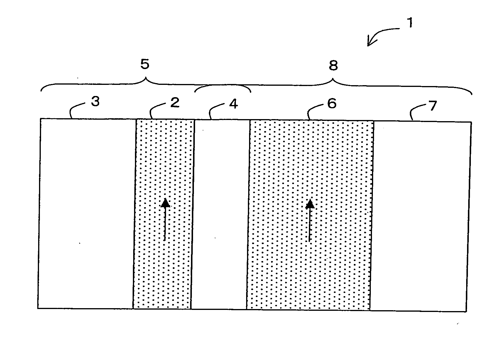
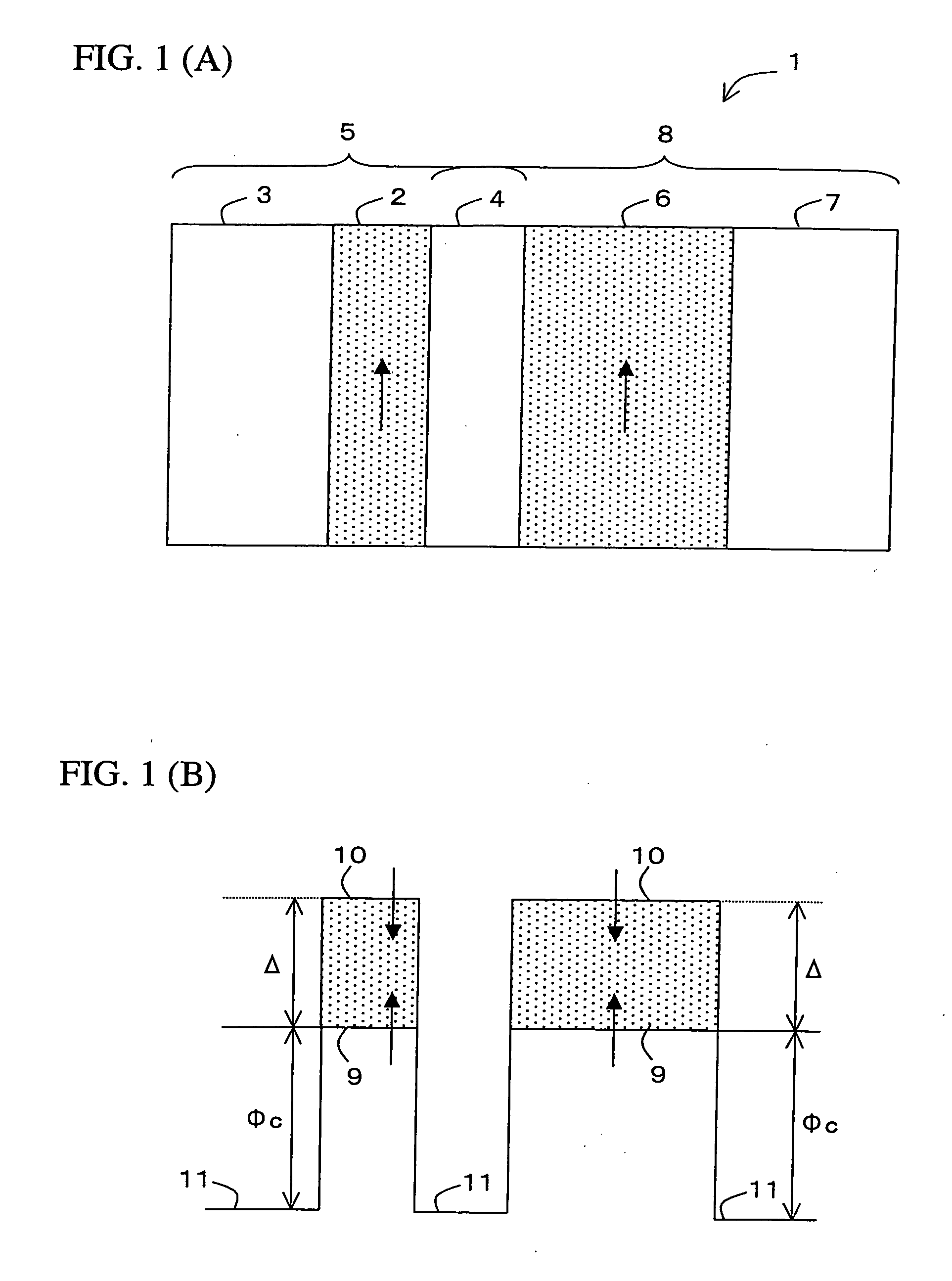
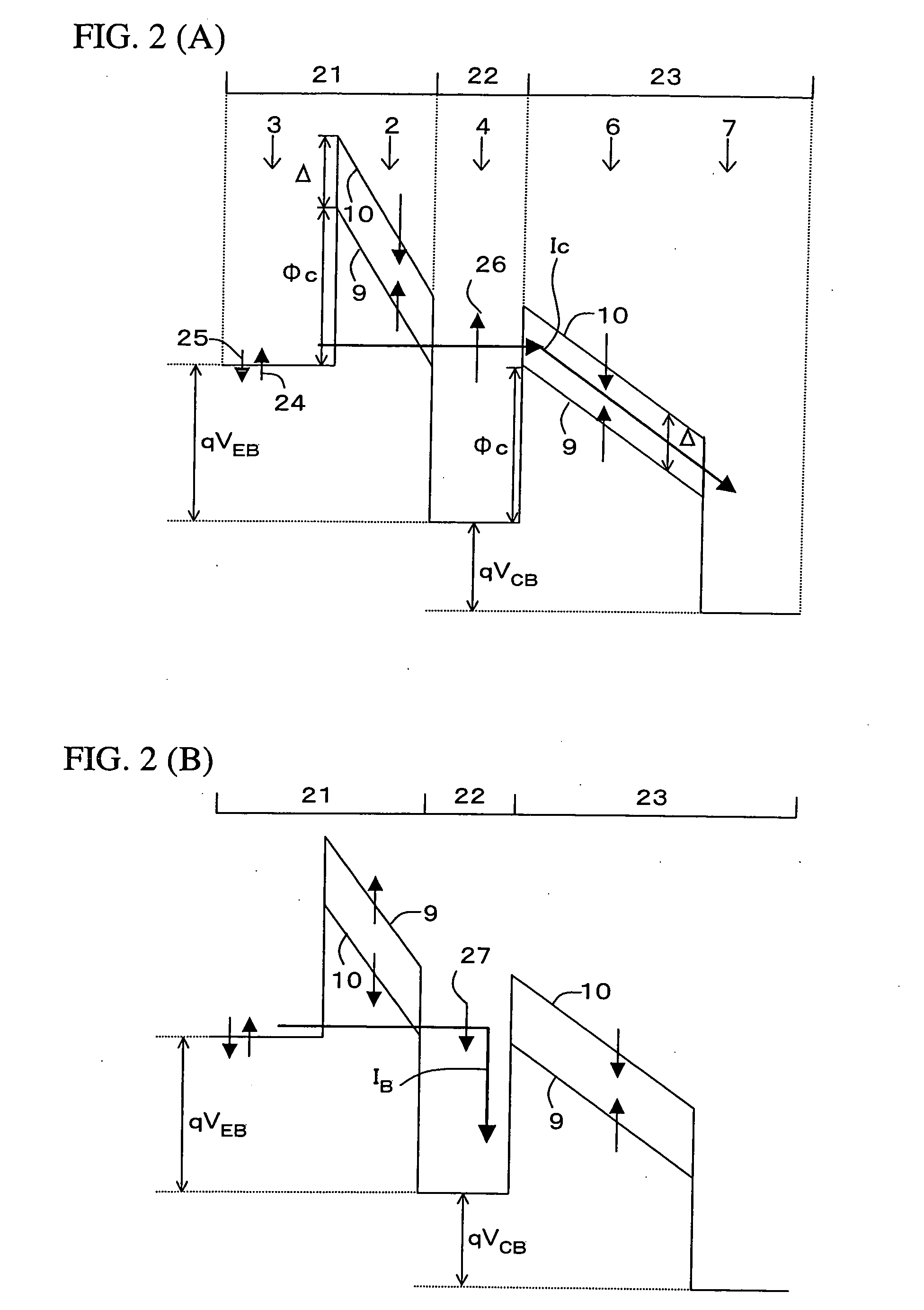
[0051] The transistor according to the present invention comprises a spin injector for injecting spin-polarized hot carriers having a specific spin direction, and a spin analyzer for selecting the thus injected spin-polarized hot carries by their spin directions. The spin injector comprises a first ferromagnetic barrier layer with such a thickness allowing for tunneling, such as Fowler-Nordheim tunneling or a direct tunneling; a first nonmagnetic electrode layer joined to one end surface of the first ferromagnetic barrier layer; and a second nonmagnetic electrode layer joined to the other end surface of the first ferromagnetic barrier layer. The spin analyzer comprises a second ferromagnetic barrier layer; a second nonmagnetic electrode layer joined to one end surface of the second ferromagnetic barrier layer; and a third nonmagnetic electrode layer joined to the other end surface of the second ferromagnetic barrier layer. The second nonmagnetic electrode layer is common to the spin...


PUM


Abstract

A spin transistor comprises a spin injector for injecting, from a first nonmagnetic electrode carriers with a spin parallel to a spin band forming the band edge of a first ferromagnetic barrier layer, to a second nonmagnetic electrode layer, as hot carriers. It also comprises a spin analyzer whereby, due to spin-splitting at the band edge of a second ferromagnetic barrier layer, the spin-polarized hot carriers are transported to a third nonmagnetic electrode when the direction of the spin of the carriers injected into the second nonmagnetic electrode is parallel to that of the spin of the spin band at the band edge of the second ferromagnetic barrier layer, whereas the hot carriers are not transported to the third nonmagnetic electrode in the case of antiparallel spin. A memory element is also provided that comprises such a spin transistor.

Description

TECHNICAL FIELD [0001] The present invention relates to a novel transistor, and more particularly to a transistor the output characteristics of which depend on the direction of spin of a carrier, and to a nonvolatile memory circuit (nonvolatile memory) utilizing the transistor. BACKGROUND ART [0002] Conventionally, semiconductor memories used in electronic devices such as microcomputers have mainly employed dynamic random access memories (DRAMs) from the viewpoint of operating speed and the degree of device integration. It is difficult, however, for DRAMs to accommodate the recent demands for lower energy consumption and mobility because DRAMs consume energy for memory storage purposes and the stored data is lost once power supply is turned off. In order to address such demands, a novel memory is required that is nonvolatile as well as fast, highly integrated, and energy-saving. [0003] Magnetoresistive random access memories (MRAMs) are now gaining attention as a next-generation mem...

Claims


Application Information

Patent Timeline
Patent Type & Authority Applications(United States)
IPC IPC(8): H01L29/94G11C11/15G11C11/16H01L21/8246H01L27/105H01L29/66H01L29/82H01L43/08
CPCG11C11/15G11C11/16H01L29/66984H01L43/08H01L29/778H01L29/78H01L29/73H10N50/10H01L27/105H01L29/82
Inventor SUGAHARA, SATOSHITANAKA, MASAAKI
Owner JAPAN SCI & TECH CORP
Why Eureka
Try Eureka