Stacked die packaging and fabrication method

a technology of stacked dies and fabrication methods, applied in semiconductor devices, semiconductor/solid-state device details, electrical devices, etc., can solve the problems of stacked dies, premature failure of dies within the stack, and lower yield of semiconductor packages, so as to reduce the amount of adhesive materials, reduce the amount of moisture, and increase the reliability of solder balls used in semiconductor packages with stacked dies

Active Publication Date: 2006-03-02
STATS CHIPPAC LTD
View PDF7 Cites 38 Cited by
  • Summary
  • Abstract
  • Description
  • Claims
  • Application Information

AI Technical Summary

Benefits of technology

[0018] The present invention provides the ability to facilitate the design of semiconductor packages in which at least one die overlies another die or a plurality of other active or passive components.
[0025] Furthermore, the reliability of solder balls used in semiconductor packages having stacked dies is increased.

Problems solved by technology

Despite efforts to overcome problems resulting in lower yields of semiconductor packages with stacked dies problems still exist.
In particular, dies within the stack fail prematurely.
Additionally, at least one die often overlies a plurality of other active or passive components making designing of such semiconductor packages more difficult.
Furthermore, the layout of bonding pads on the substrate is difficult resulting in bonding wires of various lengths being used.
Also, an upper die can crack during wire bonding of the upper die due to lack of vertical support if the upper die overhangs the next lower die in the stack of dies.
Heat dissipation in semiconductor packages having multiple dies also is a problem.
The more dies that are placed in a semiconductor package, the greater the problem with heat dissipation.
The presence of multiple dies in a semiconductor package also causes problems with the flow of the molding compound used to encapsulate the dies in forming the semiconductor package.
There also is a problem with designing suitable electrical ground paths to the dies in a stacked die semiconductor package.
Adhesive materials have the tendency to absorb moisture, which can have adverse effects on the dies that reduce the reliability and useful life of the semiconductor package.
Furthermore, there is a thermal mismatch between the materials used to position the stacked dies in the semiconductor package and the substrate.
The resulting relative motion of the dies with respect to the substrate has an adverse effect on the reliability of solder balls used to wire-bond the dies to the substrate.
Solutions to these problems have been long sought but prior developments have not taught or suggested any solutions and, thus, solutions to these problems have long eluded those skilled in the art.

Method used


Image

  • Stacked die packaging and fabrication method
  • Stacked die packaging and fabrication method
  • Stacked die packaging and fabrication method

Examples


Embodiment Construction

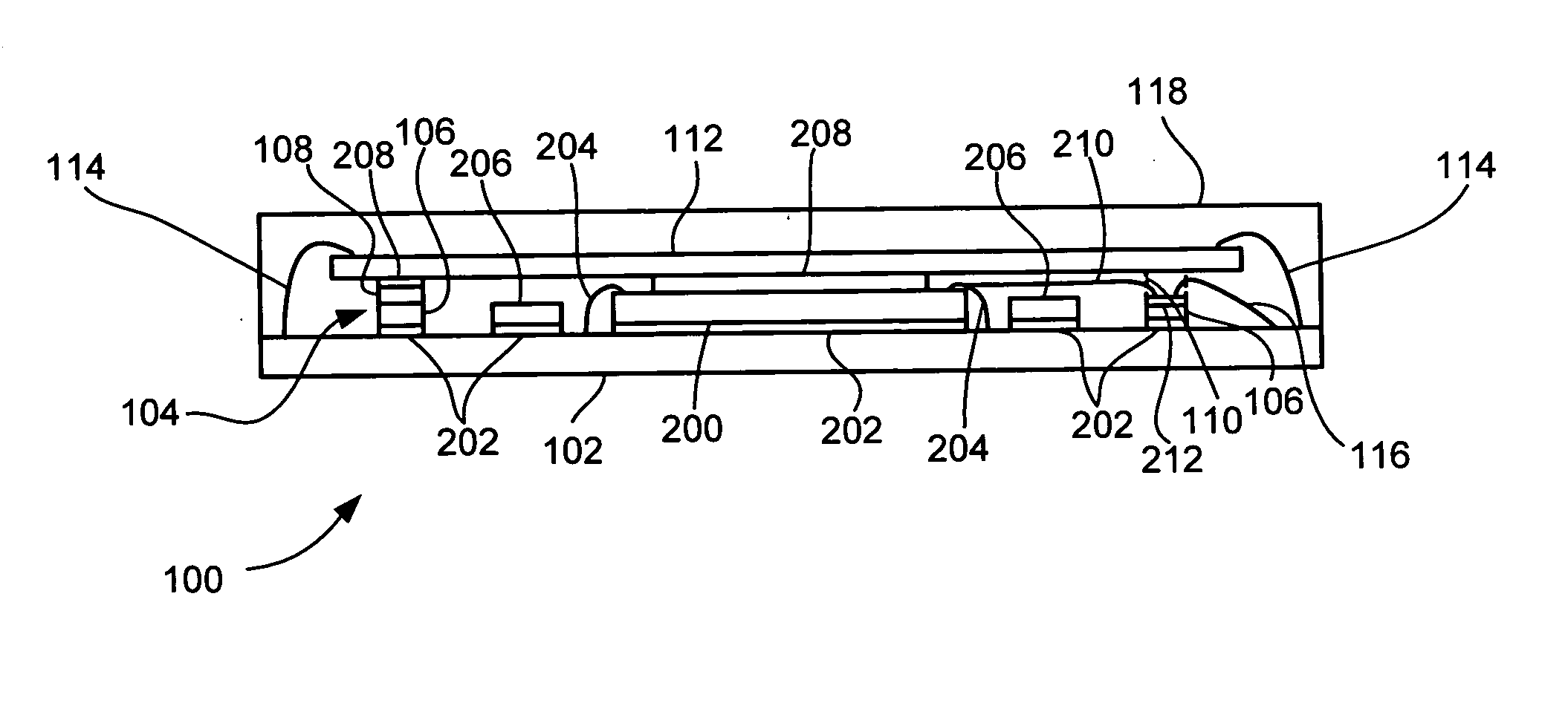
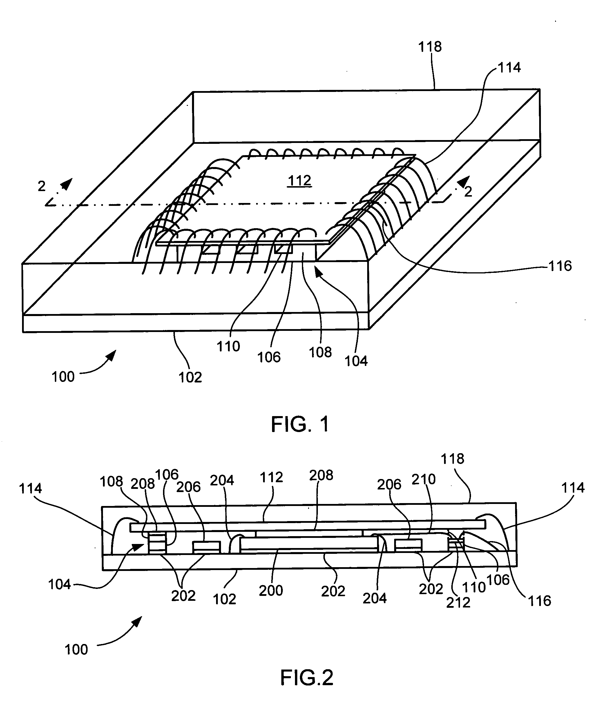
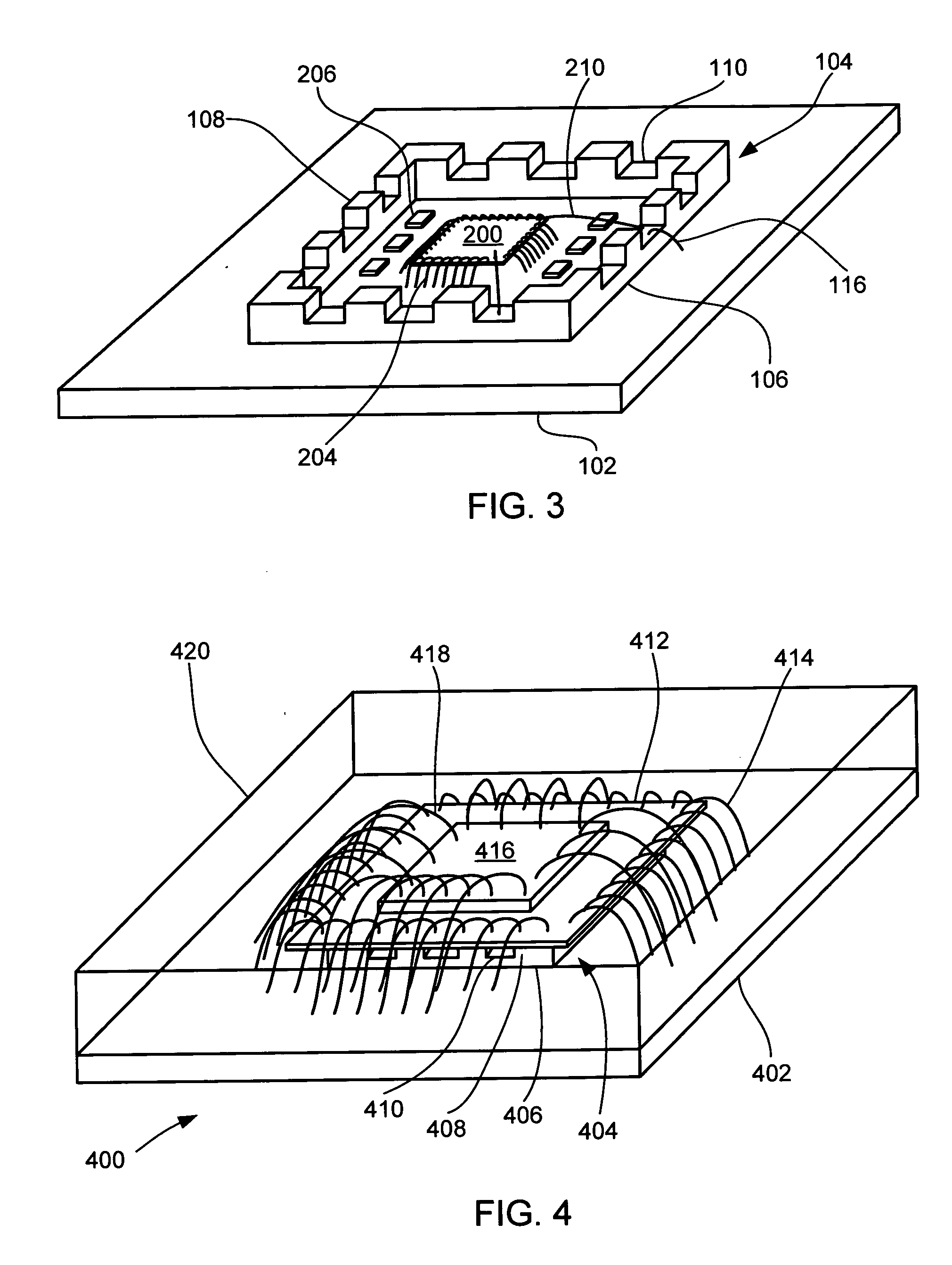
[0037] In the following description, numerous specific details are given to provide a thorough understanding of the invention. However, it will be apparent that the invention may be practiced without these specific details. In order to avoid obscuring the present invention, some well-known circuits, system configurations, and process steps are not disclosed in detail.

[0038] The drawings showing embodiments of the apparatus / device are semi-diagrammatic and not to scale and, particularly, some of the dimensions are for the clarity of presentation and are shown greatly exaggerated in the FIGs. Generally, the device can be operated in any orientation.

[0039] The term “horizontal” as used herein is defined as a plane parallel to the conventional plane or surface of the substrate, regardless of its orientation. The term “vertical” refers to a direction perpendicular to the horizontal as just defined. Terms, such as “on”, “above”, “below”, “bottom”, “top”, “side” (as in “sidewall”), “high...


PUM


Abstract

A semiconductor package includes a substrate. A crenellated spacer is attached to the substrate. At least one top die is attached to the crenellated spacer. The at least one top die is wire bonded to the substrate, and an encapsulant is formed over the crenellated spacer and the at least one top die.

Description

TECHNICAL FIELD [0001] The present invention relates generally to semiconductor devices, and more particularly, to multi-chip semiconductor packages that have stacked dies. BACKGROUND ART [0002] Semiconductors, or computer chips, have made their way into virtually every electrical product manufactured today. Chips are used not only in very sophisticated industrial and commercial electronic equipment, but also in many household and consumer items such as televisions, clothes washers and dryers, radios and telephones. As many of these types of products become smaller but more functional, there is a need to include more chips in these smaller products. The reduction in size of cellular telephones is one example of how more and more capabilities find their way into smaller and smaller electronic products. [0003] As the demand for semiconductor devices with low-cost, high performance, increased miniaturization, and greater packaging densities has increased, Multi-Chip Module (MCM) struct...

Claims


Application Information

Patent Timeline
Patent Type & Authority Applications(United States)
IPC IPC(8): H01L23/02
CPCH01L23/3121H01L24/48H01L25/0657H01L25/50H01L2224/32145H01L2224/48091H01L2224/48227H01L2224/73265H01L2225/0651H01L2225/06575H01L2225/06582H01L2924/01079H01L2924/19041H01L2924/19105H01L2924/30107H01L2924/19103H01L2224/32225H01L25/0652H01L2924/00014H01L2924/00012H01L24/73H01L2924/181H01L2224/73257H01L2224/45124H01L2224/45144H01L24/45H01L24/49H01L2224/49175H01L2224/45015H01L2924/207
Inventor CHOW, SENG GUANYING, MINGSHIM, IL KWONEMIGH, ROGER
Owner STATS CHIPPAC LTD
Why Eureka
Try Eureka