Circuit device and manufacture method for circuit device

a circuit device and manufacturing method technology, applied in the field of circuit devices, can solve the problems of insufficient cost, space and connection reliability, weak vibration resistance, and product compactness, and achieve the effects of low cost, less mutual interference, and good yield

Inactive Publication Date: 2006-03-02
SONY CORP
View PDF14 Cites 51 Cited by
  • Summary
  • Abstract
  • Description
  • Claims
  • Application Information

AI Technical Summary

Benefits of technology

[0027] According to the manufacture method for a circuit device of the embodiment of the present invention configured as above, on both sides of the insulating sheet, the conductive wiring patterns such as plated copper and conductive paste are formed by a photolithography method or a printing method, and after the wiring patterns on both sides are electrically connected, the electronic components are mounted to thereby form the plurality of circuit blocks. In this case, the circuit blocks are electrically connected by the first wiring patterns disposed on one side of the insulating sheet. Accordingly, by folding the plurality of circuit blocks at the first wiring patterns and filling the insulating resin having the electromagnetic shielding effects between the plurality of circuit blocks and curing the insulating resin, it becomes possible to manufacture a circuit device with less mutual interferences between mounted electronic components.
[0028] According to the circuit device and the manufacture method for a circuit device of embodiments of the present invention, it is possible to conduct a performance test, for example, an operation test or the like when electro...

Problems solved by technology

Connectors are unsatisfactory in that they raise cost, and since mount spaces are required for wiring boards, products have a disadvantage in compactness and is weak against vibrations and the like.
Although there is a thin connector using a flexible cable, this is not satisfactory in cost, space and connection reliability.
However, if a circuit sensitive to electromagnetic interferences or the like is mounted, electromagnetic interf...

Method used


Image

  • Circuit device and manufacture method for circuit device
  • Circuit device and manufacture method for circuit device
  • Circuit device and manufacture method for circuit device

Examples


Embodiment Construction

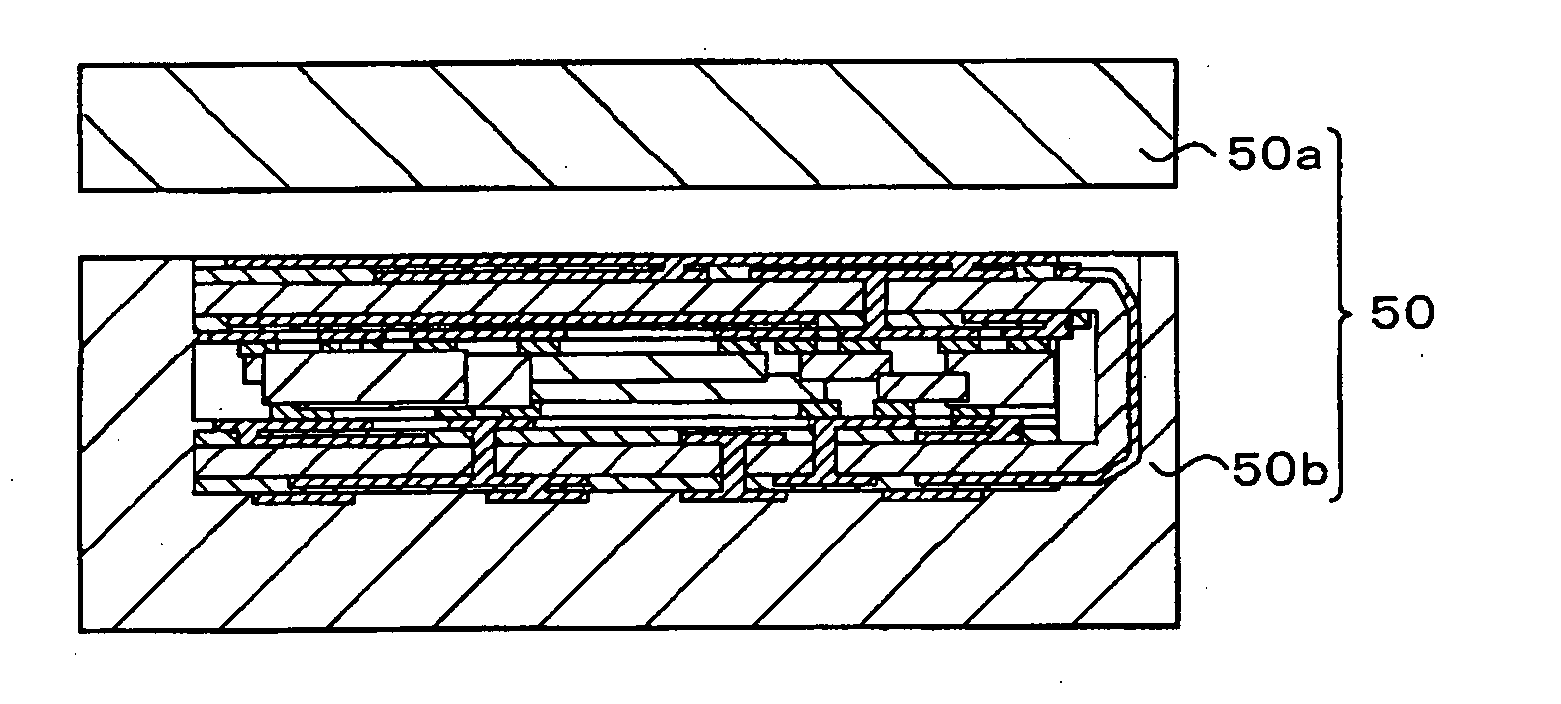
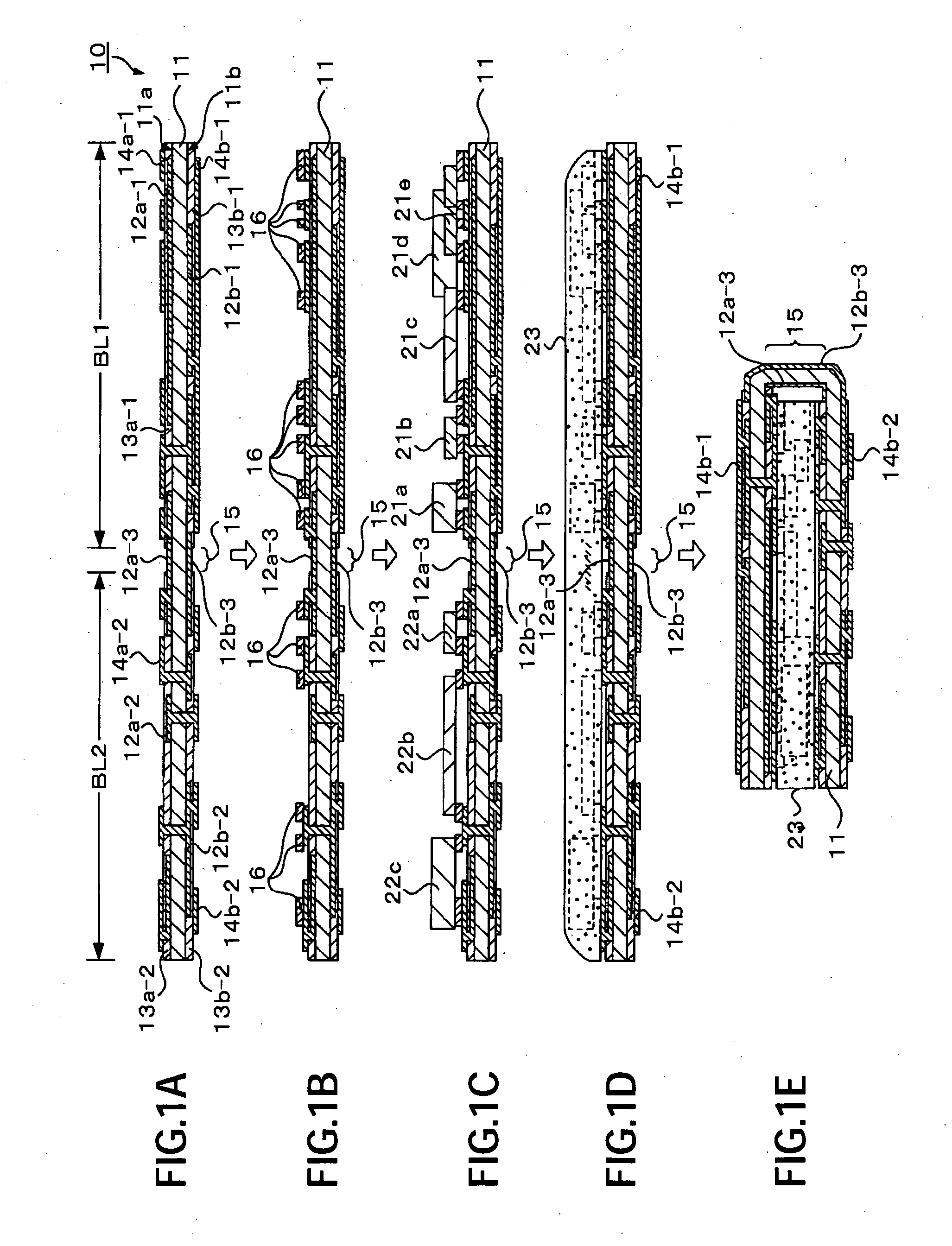
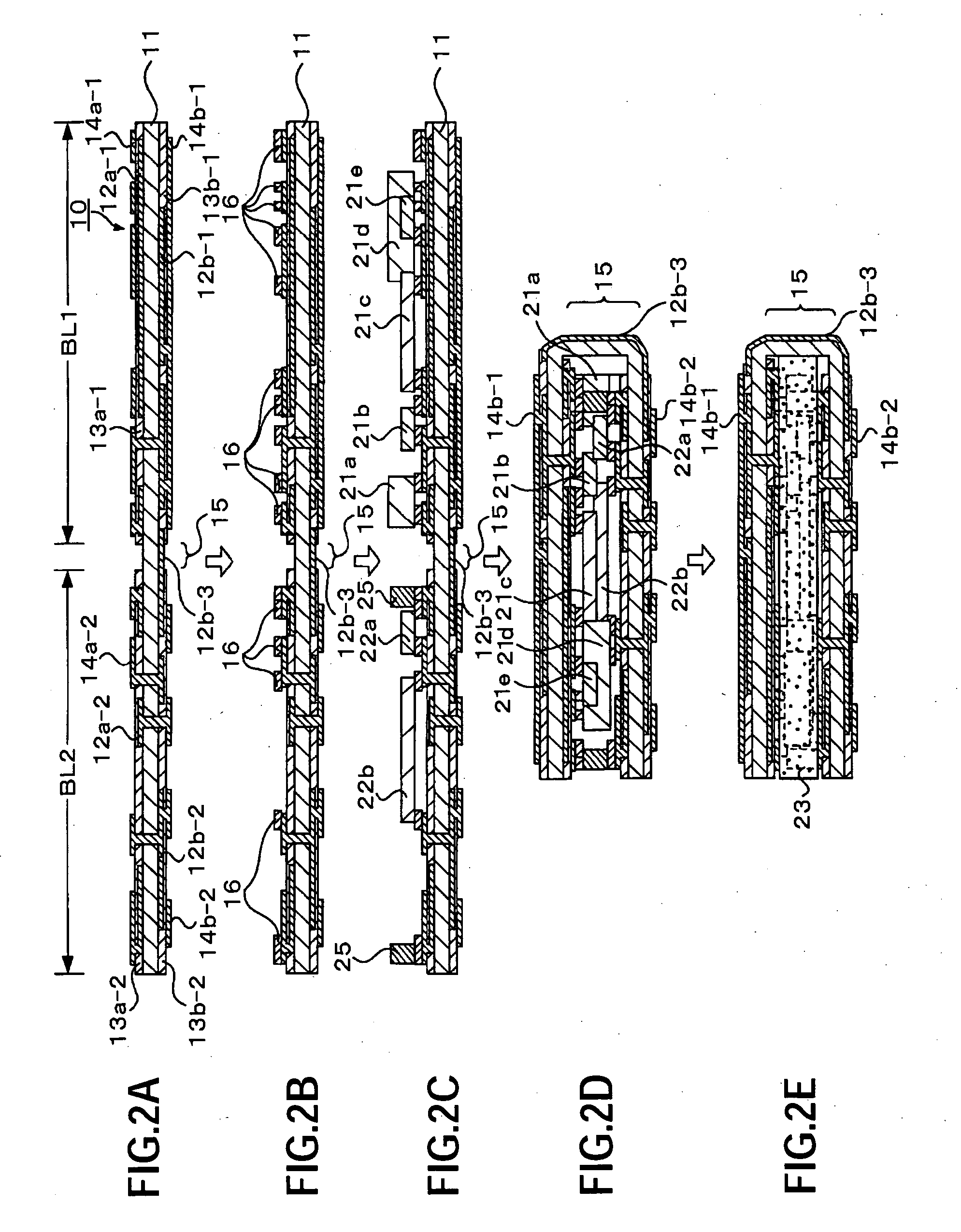
[0036] With reference to FIGS. 1A to 1E, description will be made on a preferred embodiment of a circuit device and a manufacture method for a circuit device of the present invention.

[0037]FIGS. 1A to 1E are manufacture process flow diagrams illustrating a manufacture method for a circuit device according to the embodiment. The circuit device is manufactured by using a four-layer flex-rigid board as a base member.

[0038]FIG. 1A is a cross sectional view of a four-layer flex-rigid board, FIG. 1B is a cross sectional view of the board after conductive paste is coated, FIG. 1C is a cross sectional view of the board after electronic components are mounted, FIG. 1D is a cross sectional view of the board after insulating resin is coated, and FIG. 1E is a cross sectional view of the circuit device formed through folding and curing.

[0039] In FIGS. 1A to 1E, reference numeral 10 represents the four-layer flex-rigid board, reference numeral 11 represents a polyimide sheet made of polyimide ...


PUM


Abstract

There is provided a circuit device including a plurality of circuit blocks, wherein: on one surface of an insulating sheet having flexibility, a first and a second wiring patterns are formed, the second wiring pattern including a plurality of divisionally disposed patterns and electrically connected to the first wiring pattern; in an area corresponding to the second wiring pattern on another surface of the insulating sheet, a third wiring pattern including a plurality of patterns is formed and electrically connected to the second wiring pattern via a conductive hole; electronic components are mounted on the third wiring pattern so as to form the divisionally disposed circuit blocks; the plurality of circuit blocks are folded by directing the electronic component mounting surface of the insulating sheet inward and the second wiring pattern outward; and insulating resin having electromagnetic shielding effect is filled in gaps between the plurality of folded circuit blocks.

Description

BACKGROUND OF THE INVENTION [0001] 1. Field of the Invention [0002] The present invention relates to a circuit device using a plurality of circuit blocks connected together without connectors and being particularly suitable for high frequency use and to a manufacture method for the circuit device of this type. [0003] 2. Description of Related Art [0004] As a conventional method of connecting, e.g., two circuit blocks, there are a method of connecting a flexible cable board between two connectors of two wiring boards mounting each circuit block, a method of mounting two circuit blocks on a wiring board having not a connector but a flexible part and mounting the wiring board in a narrow space of a product by utilizing flexibility of the flexible part, and other methods. These methods are generally adopted in assembling electric products. A method is disclosed as an example of the latter in Japanese Patent Unexamined Publication No. 2001-358422 (FIG. 5). [0005] Furthermore, for example...

Claims


Application Information

Patent Timeline
IPC IPC(8): H01L23/02H01L23/52H01L21/50H01L21/48H01L21/44
CPCH01L23/5387H01L23/552H01L25/0652H01L2224/16H01L2924/01078H01L2924/3025H05K2201/086H05K1/189H05K3/284H05K3/4626H05K3/4647H05K2201/055H05K1/0233H01L2924/00014H01L2924/00011H01L2224/0401H05K1/14H05K1/11
Inventor WATANABE, YOSHIO
Owner SONY CORP
Why Eureka
Try Eureka