Plasma display panel, method of driving same and plasma display apparatus
a plasma display panel and plasma display technology, applied in the direction of instruments, static indicating devices, gas discharge vessels/containers, etc., can solve the problem of limited degree to which the pixel pitch can be reduced, the scale of the drive circuit must be large, and the stumbling block to achieve high definition. achieve the effect of increasing the number of gradations and increasing the brightness
- Summary
- Abstract
- Description
- Claims
- Application Information
AI Technical Summary
Benefits of technology
Problems solved by technology
Method used
Image
Examples
first embodiment
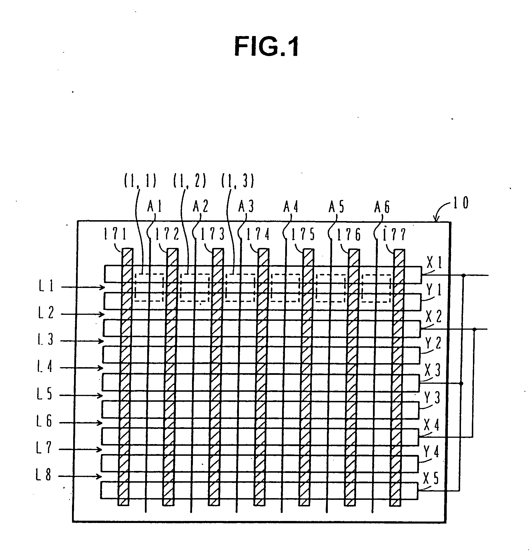
[0082]FIG. 1 shows a PDP 10 in the first embodiment according to the present invention. In FIG. 1, pixels are indicated with dotted lines only for display line L1. In order to simplify the explanation, the number of pixels of the PDP 10 is 6×8=48 monochromatic pixels. The present invention may be applied to both color and monochromatic pixels and three monochromatic pixels corresponds to one color pixel.
[0083] In order to facilitate production and to achieve higher definition by reducing the pixel pitch, the PDP 10 has a structure in which the partitioning walls 191 to 199 in the PDP 10Q in FIG. 31 are removed. In order to ensure that erroneous discharge does not occur among adjacent display lines due to the removal of the partitioning walls, interlaced scanning is performed in such a manner that the phases of the waveforms of the sustaining pulse voltages in the odd-numbered lines and in the even-numbered lines among the electrodes L1 to L8, which perform surface discharge and wil...
second embodiment
[0129] If the number of pulses can be reduced in FIGS. 7 and 8, power consumption can also be reduced. During an address period, if the pulses supplied to the odd-numbered X electrodes and the even-numbered X electrodes are made to be continuous, the number of pulses can be reduced. This can be achieved by performing scanning in the order shown in FIG. 6(B). To be more specific, the display lines L1, L3 / L5 and L7 in the odd-numbered field should be further divided into odd-numbered lines and even-numbered lines and after scanning one group sequentially, the other group should be scanned sequentially. The same procedure is performed for the even-numbered field.
[0130]FIG. 9 shows the schematic structure of a plasma display apparatus 20A in the second embodiment for implementing this method.
[0131] During an address period, in order to perform scanning in the order of the electrodes Y1, Y3, Y2 and Y4, the output of the driver 232(2) is connected to the electrode Y3 and the output of a...
third embodiment
[0134] In FIG. 7, the common pulse at the voltage Vx is supplied to the electrodes X1, X3 and X5 and the common pulse at the voltage Vx is supplied to the electrodes X2 and X4. However, it suffices to supply a pulse at the voltage Vx to the electrodes X1 to X4 selected sequentially when the electrodes Y1 to Y4 are selected sequentially. In this way, the number of pulses supplied to the electrodes is reduced and power consumption is also reduced.
[0135] To achieve the above in a plasma display apparatus 20B in the third embodiment, a scanning circuit 30 is provided for the X electrodes, too, as shown in FIG. 12. The scanning circuit 30 is different from the scanning circuit 23 only in that the number of components is larger by the equivalent of one electrode.
[0136] During an address period, “1” is provided to the data input for bit 301 (1) in the odd-numbered field and “1” is provided to the data input for bit 301(2) in the even-numbered field at a shift register 301 from a control ...
PUM
 Abstract
Description
Claims
Application Information


