Jitter-resistive delay lock loop circuit for locking delayed clock and method thereof

a delay lock and loop technology, applied in the direction of electrical appliances, pulse automatic control, etc., can solve the problems of jitter, erroneous delay clocks, and little delay provided by dll, so as to reduce resist jitter, and alleviate the effect of jitter

Inactive Publication Date: 2006-03-16
MEDIATEK INC
View PDF3 Cites 7 Cited by
  • Summary
  • Abstract
  • Description
  • Claims
  • Application Information

AI Technical Summary

Benefits of technology

[0012] It is one advantage of this invention that the present invention DLL is capable of resisting the jitter. This solution is the combined effects of a clock divider and a 180° phase detector. The clock divider makes a frequency-divided clock have a longer clock cycle and lower frequency, which tends to alleviate the effects of jitter. The 180° phase detector further reduces the effects of jitter by detecting the 180° phase difference once. This means, that if the serious jitter occurs after one 180° phase difference detected, the jitter shifting a next rising or falling edge does not interfere with the operation of the DLL.

Problems solved by technology

That is, the DLL provides an amount of delay that appropriately shifts the original rising and falling edges of the memory clock.
However, the DLL 10 shown in FIG. 1 does little to resist the effects of jitter.
Jitter is typically caused by electromagnetic interference and cross talk with other signals.
The effect of jitter on the DLL 10 results in erroneous delayed clocks, thereby making the DLL 10 malfunction to lock a wrong phase difference.
As a result, each delay cell 13 does not provide a wanted amount of delay equaling T / K.
Therefore, an application device is unable to function normally due to an improper delayed clock generated from the delay line 12 of the related art DLL 10.

Method used


Image

  • Jitter-resistive delay lock loop circuit for locking delayed clock and method thereof
  • Jitter-resistive delay lock loop circuit for locking delayed clock and method thereof
  • Jitter-resistive delay lock loop circuit for locking delayed clock and method thereof

Examples


Embodiment Construction

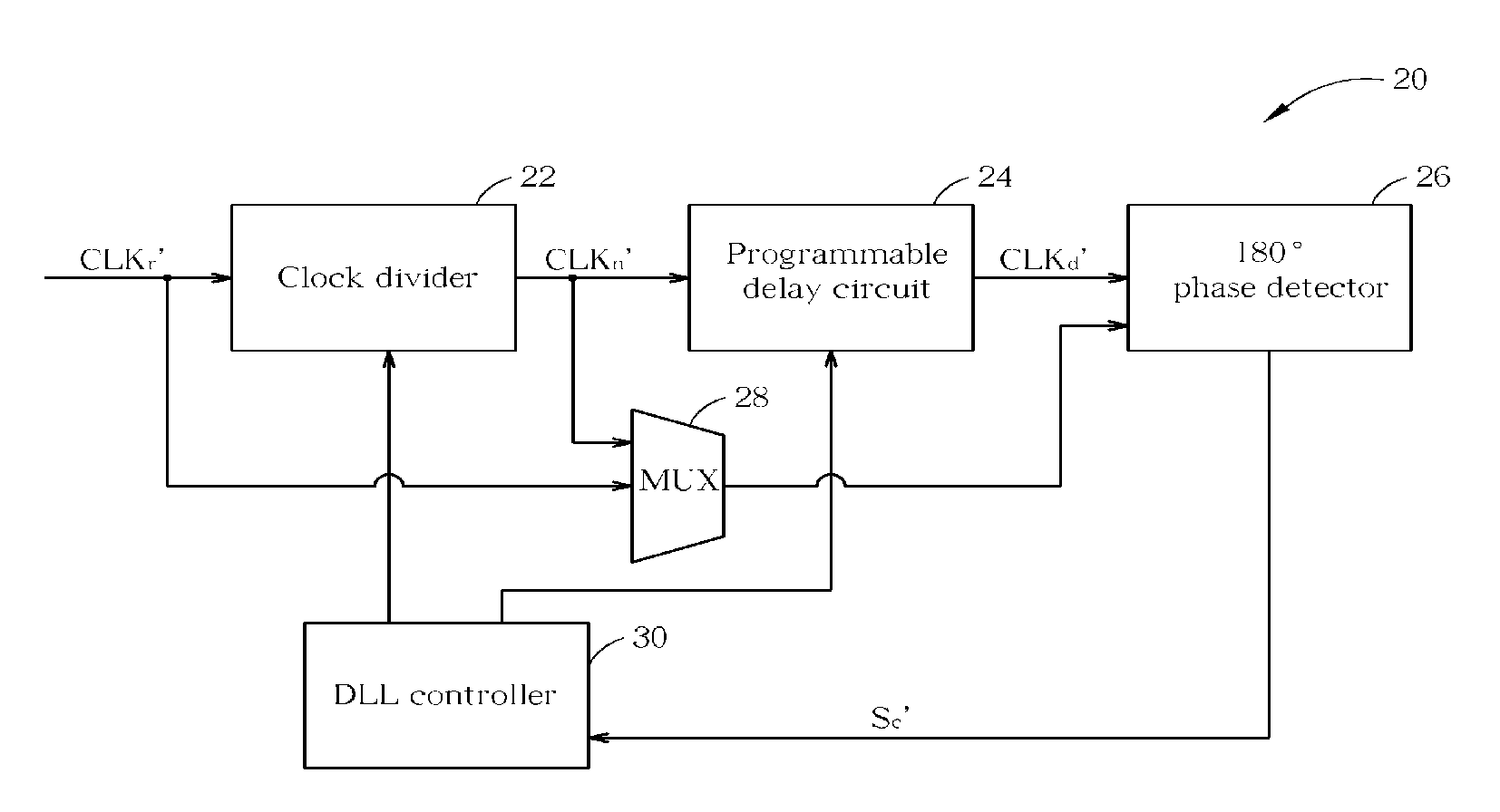
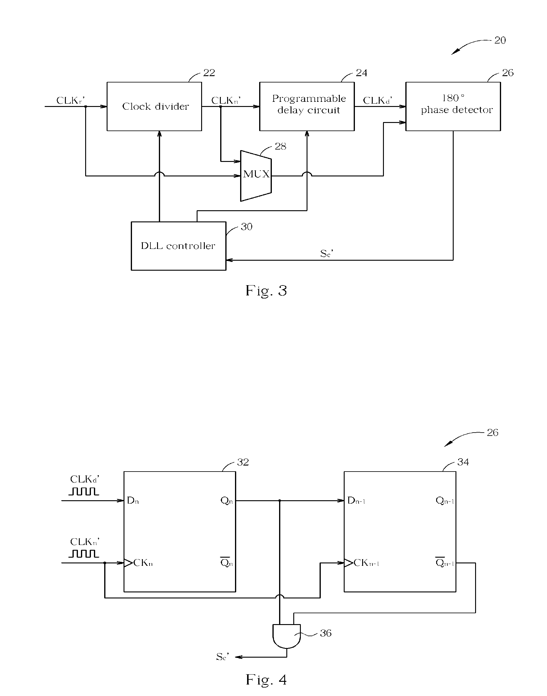
[0020]FIG. 3 is a block diagram of a digital DLL 20 according to a first embodiment of the present invention. The DLL 20 comprises a clock divider 22, a programmable delay circuit 24, a 180° phase detector 26, a multiplexer (MUX) 26 and a DLL controller 30. In the configuration shown in FIG. 3, the DLL 20 is capable of resisting the effects of jitter. A reference clock CLKr′ is inputted into the clock divider 20, which divides the frequency of the reference clock CLKr′ by a frequency-dividing value D and generates a frequency-divided clock CLKn′. The frequency-dividing value D can be specified by the user in the DLL controller 30 and is passed to the clock divider 20. That is, the frequency-dividing value D is programmable and dictated by the intended application of the DLL 20. The division of the frequency of CLKr′ is partially responsible for resisting the effects of jitter; this will be described in greater depth later.

[0021] Generally speaking, the division of frequency is made...


PUM


Abstract

A delay lock loop circuit for delaying a reference clock to lock a delayed clock. The delay lock loop circuit includes a clock divider for dividing a frequency of the reference clock by N to generate a frequency-divided clock, a programmable delay circuit electrically coupled to the clock divider for delaying the frequency-divided clock to generate the delayed clock, a 180° phase detector electrically coupled to the programmable delay circuit for detecting a phase change of the delayed clock, and a delay lock loop controller electrically coupled to the programmable delay circuit and the 180° phase detector for programming the programmable delay circuit to lock the delayed clock according to the phase change.

Description

BACKGROUND OF INVENTION [0001] 1. Field of the Invention [0002] The invention relates to a delay lock loop (DLL) circuit and related method, and more particularly, to a jitter-resistive digital DLL circuit and related method for delaying a reference clock to lock a delayed clock through detecting one phase change. [0003] 2. Description of the Prior Art [0004] Delay lock loop (DLL) circuitry is commonly utilized in computer processing environments for generating a required clock. While the clock rate of computers continually is increasing, low-skew clock distributions are becoming more important to achieve design speed objectives. Related art computer systems include processors that exchange data with a variety of memory devices and input / output peripheral devices. An exemplary memory device is a synchronous dynamic random access memory (SDRAM) employing a pipelined data to be transferred to the processor at a data transfer rate which is comparable to the processor's operating freque...

Claims


Application Information

Patent Timeline
Patent Type & Authority Applications(United States)
IPC IPC(8): H03L7/06
CPCH03L7/085H03L7/0814H03L7/0816
Inventor TSENG, JUI-HSING
Owner MEDIATEK INC
Why Eureka
Try Eureka