Antenna switch circuit and high frequency module having the same

a switch circuit and high frequency module technology, applied in the field of antenna switch circuits, can solve the problems of signal leakage at a cross point that may further leak to the receiving signal line, and achieve the effect of reducing leakage, reducing insertion loss, and effectively reducing leakag

Active Publication Date: 2006-03-23
RENESAS ELECTRONICS CORP
View PDF2 Cites 12 Cited by
  • Summary
  • Abstract
  • Description
  • Claims
  • Application Information

AI Technical Summary

Benefits of technology

[0007] The antenna switch circuit is typically formed by an integrated circuit. As the integration of an integrated circuit is increased, the gap between these signal lines at a cross point becomes narrower. Since an interlayer insulating film is formed at the cross point, a capacitance is formed between the signal lines with the interlayer insulating film acting as a dielectric material. The higher the frequency, the more notable the effect of this capacitance. If transmitting high frequency signals leak through this combined capacitance, power efficiency will be reduced. If receiving high frequency signals leak, receiving sensitivity will be lowered. Moreover, signals that leaked at a cross point may further leak to the receiving signal lines via other cross points or other switch devices.
[0015] According to the present invention, current leakage is suppressed by the resistive elements which are disposed away from and across the cross point, not at the cross point, and thereby signal leakage can be effectively reduced.

Problems solved by technology

Moreover, signals that leaked at a cross point may further leak to the receiving signal lines via other cross points or other switch devices.

Method used


Image

  • Antenna switch circuit and high frequency module having the same
  • Antenna switch circuit and high frequency module having the same
  • Antenna switch circuit and high frequency module having the same

Examples


Embodiment Construction

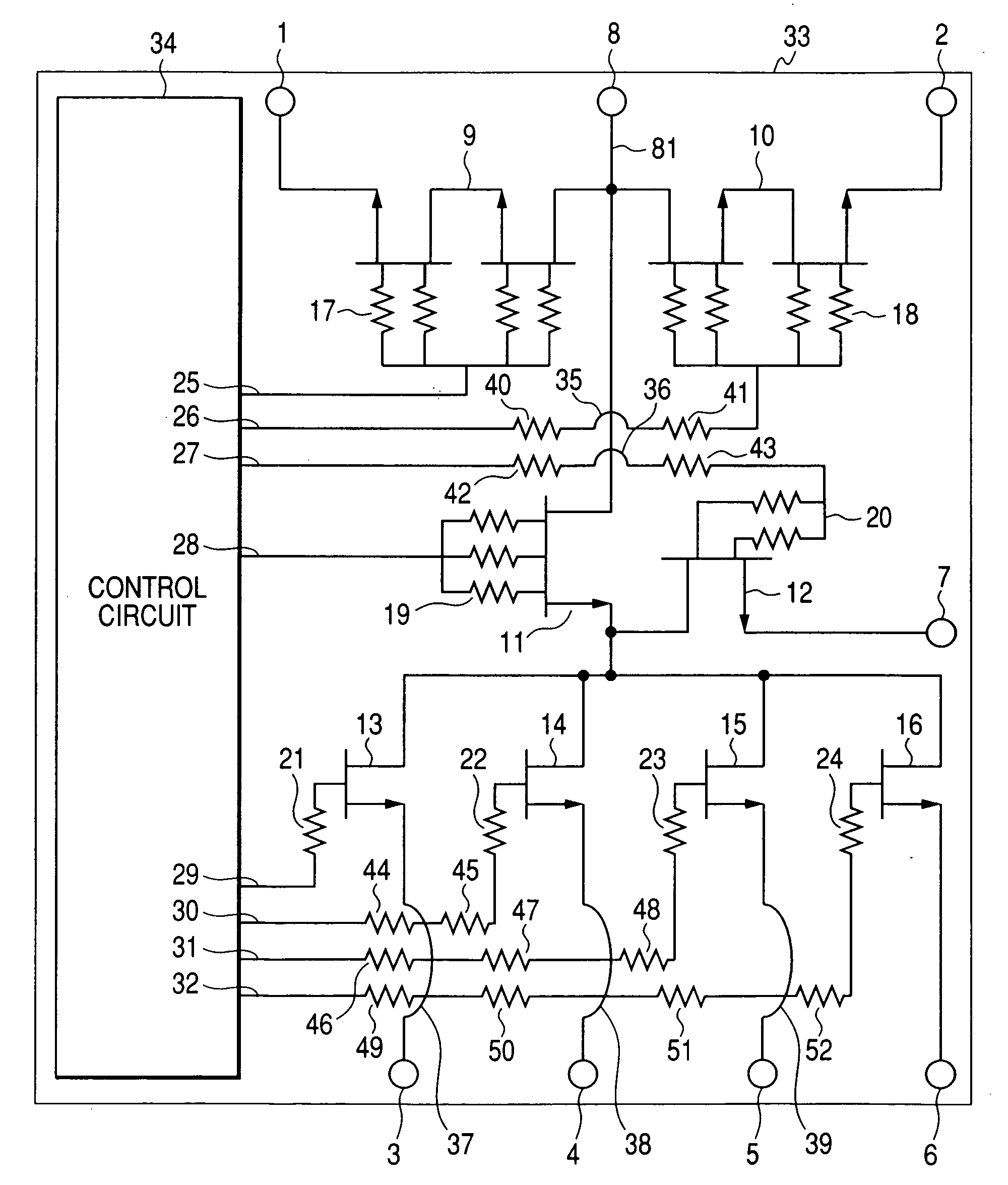
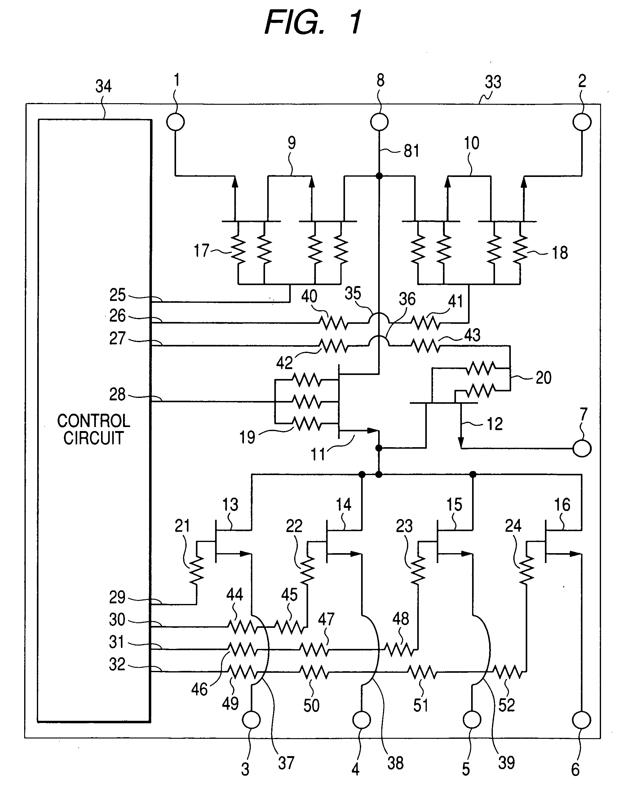
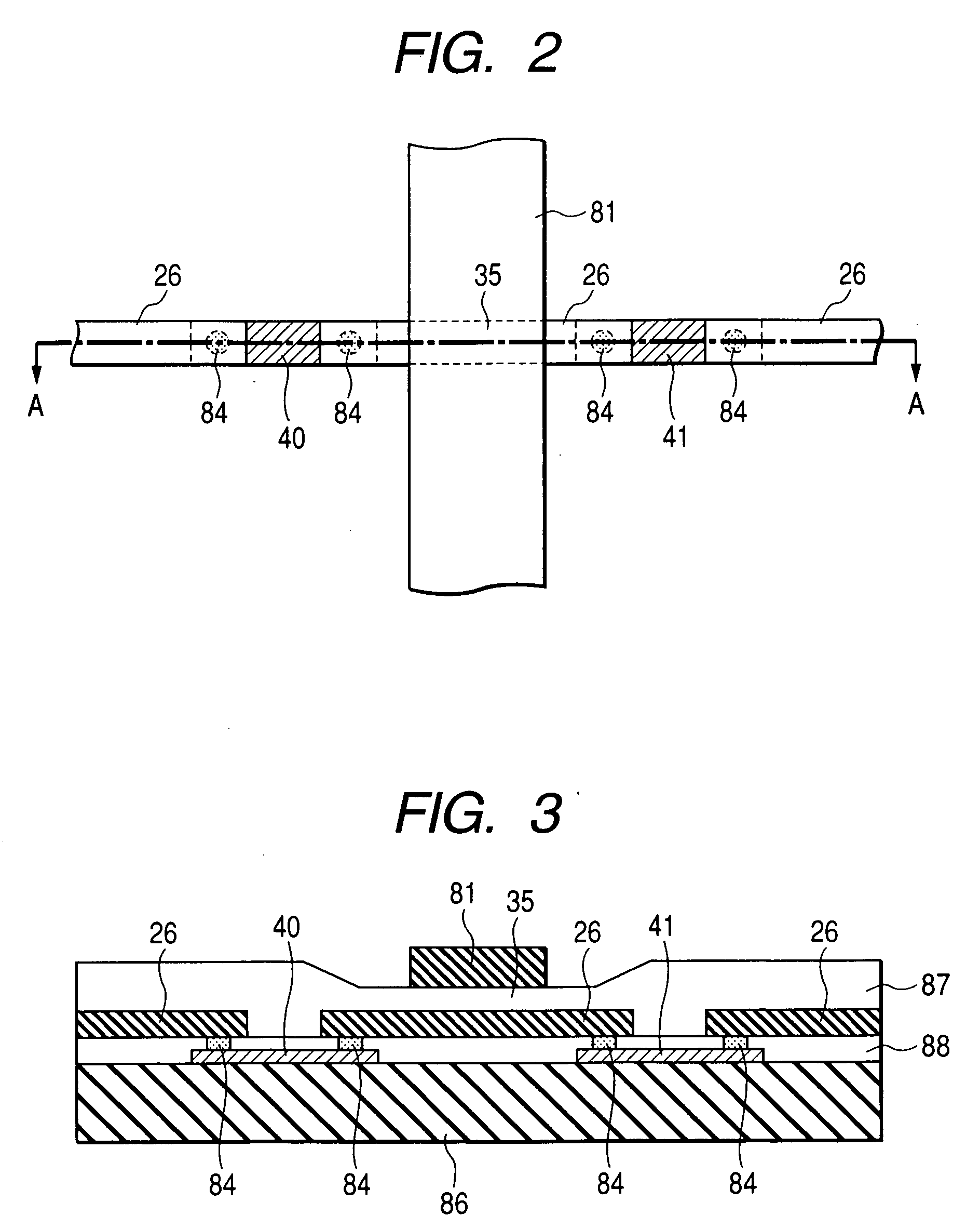
[0023] With reference to the embodiments shown in the drawings, an antenna switch circuit according to the present invention or a high frequency module containing said antenna switch circuit will be described below. The same reference numbers in FIGS. 1 to 4 denote the same or similar items, and therefore repeated descriptions of them will not be made.

[0024]FIG. 1 shows an embodiment of the antenna switch according to the present invention. In this figure, 9 and 10 denote switches (first switches) which connect transmitting terminals 1 and 2 to an antenna terminal 8 respectively, 11 is a switch which turns on when receiving and off when transmitting, 12 is a switch that turns off when receiving and on when transmitting for connection with a high frequency ground terminal 7, and 13 to 16 are switches (second switches) that connect receiving terminals 3 to 6 to the antenna terminal 8 respectively via a switch 11. Furthermore, in FIG. 1, 81 denotes a high frequency signal line (a firs...


PUM


Abstract

An object of the present invention is to provide an antenna switch circuit that effectively reduces signal leakages at a cross point even at higher operating frequencies and a high frequency module containing said antenna switch module. The antenna switch circuit comprises: a high frequency signal line to transmit a transmitting signal to be input to transmitting terminals to an antenna terminal and also to transmit a receiving signal to be input to the antenna terminal to receiving terminals; switches that are connected in the middle of the high frequency signal line between transmitting terminal and antenna terminal; switches that are connected in the middle of the high frequency signal line between receiving terminal and antenna terminal; and signal lines to transmit control signals for controlling turning on and off of the switches.

Description

CLAIM OF PRIORITY [0001] The present application claims priority from Japanese application JP 2004-271048 filed on Sep. 17, 2004, the content of which is hereby incorporated by reference into this application. FIELD OF THE INVENTION [0002] The present invention relates to an antenna switch circuit for switching the connection to a common antenna between a transmitter circuit and a receiver circuit, and a high frequency module containing said antenna switch circuit. BACKGROUND OF THE INVENTION [0003] As the circuits of a mobile phone are increasingly integrated, the thickness of a wiring substrate formed of layered dielectric plates becomes thinner. As a result, if a high frequency signal line is crossed with another signal line over a layer of the wiring substrate, both signal lines come close to each other at the cross point. [0004] At the cross point where both signal lines come close to each other, a combined capacitance is formed by both wiring layers and an insulating material ...

Claims


Application Information

Patent Timeline
Patent Type & Authority Applications(United States)
IPC IPC(8): H01P1/15
CPCH04B1/525
Inventor OGAWA, TAKASHITAKATANI, SHINICHIRONAKAJIMA, AKISHIGESHIGENO, YASUSHITANGE, EIGO
Owner RENESAS ELECTRONICS CORP
Why Eureka
Try Eureka