Packaging method, packaging structure and package substrate for electronic parts
Inactive Publication Date: 2006-03-23
FUJITSU LTD
View PDF6 Cites 6 Cited by
Summary
Abstract
Description
Claims
Application Information
AI Technical Summary
This helps you quickly interpret patents by identifying the three key elements:
Problems solved by technology
Method used
Benefits of technology
Benefits of technology
[0019] The invention was made in view of these problems and aims at providing a packaging method, a packaging structure and a package substrate capable of restraining a warp of a thin film substrate, this being done, increasing a product yield, and building up a sufficient cooling capacity in the case of mounting an electronic part having a high exothermic quantity.
[0036] Furthermore, the second substrate can be provided with a stiffener for reinforcement. In this case, even in a case where the second substrate is thin and is therefore low of its rigidity, the rigidity of the second substrate is raised by providing the stiffener. Accordingly the handleability of the second substrate is improved.
Problems solved by technology
The conventional package substrate 154 is, however, hard to ensure fixed or higher flatness due to, as shown in FIG. 21, an occurrence of warp in a thin film substrate 150 because of a low rigidity of the thin film substrate 150.
Hence, there arises a problem, wherein a product yield of the package substrate 154 is low and decreased on the order of several percents (%) as the case may be.
Method used
Image
Click on the blue label to locate the original text in one second.
Reading with bidirectional positioning of images and text.
Examples
first embodiment
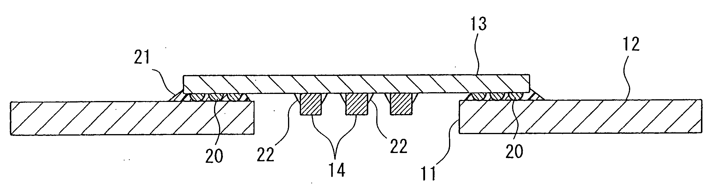
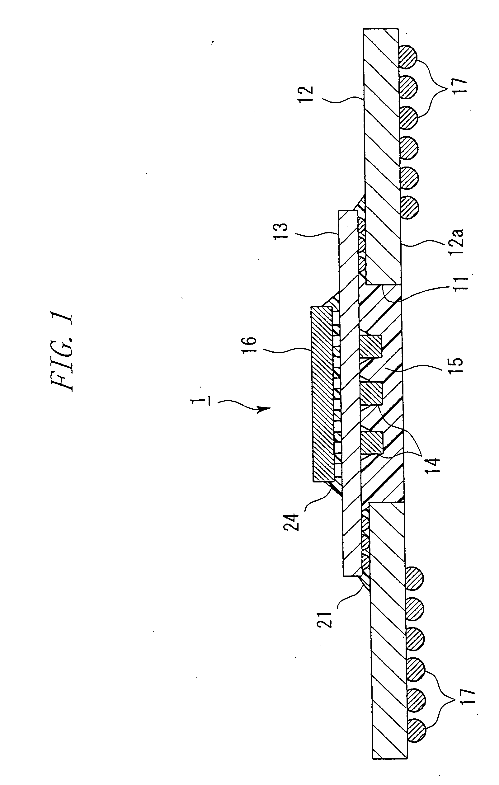
[0065]FIG. 1 is a diagram showing a package substrate 1 to which the invention is applied. This package substrate 1 includes a parent board (a first substrate) 12 having an opening 11, and a thin film substrate (a second substrate) 13 laminated on this parent board 12 in a state of covering the opening 11.
[0066] Further, this package substrate 1 includes a capacitor (a first electronic part) 14 bonded to the thin film substrate 13 and inserted into the opening 11, a hard resin 15 filling an interior of the opening 11, an LSI (Large Scale Integrated circuit, a second electronic part) 16 bonded on the surface, on the opposite side to the capacitor 14, of the thin film substrate 13, wiring (unillustrated) that connects the capacitor 14 to the LSI 16, and solder balls 17 provided on the parent board 12.
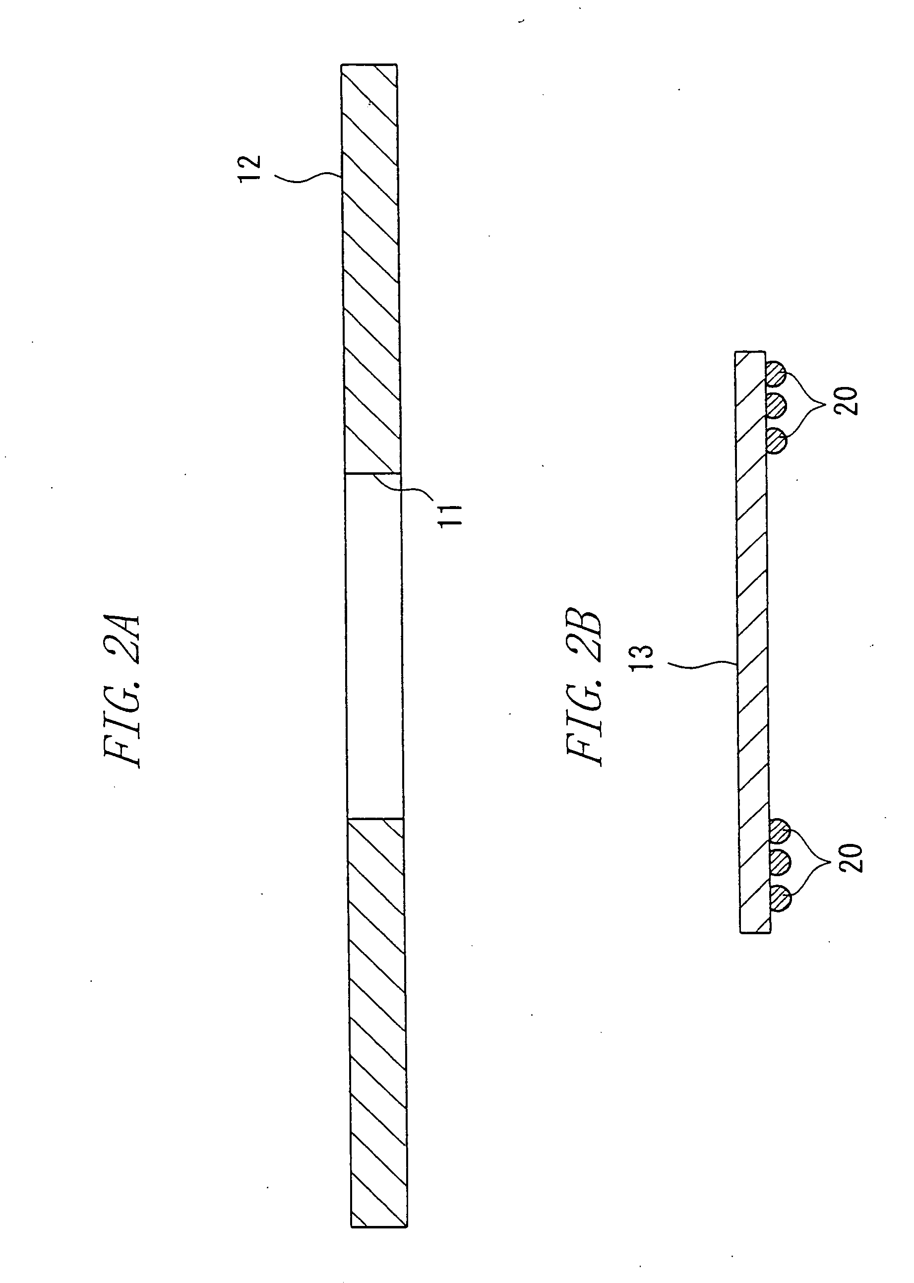
[0067] The parent board 12 may use a substrate of which a thickness is on the order of, e.g., 0.6 through 1.0 mm. Further, the thin film substrate 13 may use a substrate of which a thic...
second embodiment
[0093]FIG. 7 illustrates a package substrate 3 in a second embodiment according to the invention. In this package substrate 3, as in the package substrate 1 in FIG. 1, the resin 15 fills the interior of the opening 11 of the parent board 12.
[0094] In this package substrate 3, however, a sustaining member 30 sustaining the resin 15 is bonded to an exposed surface (a lower side in FIG. 7) of the resin 15. The portions other than this are the same as those of the package substrate 1 in FIG. 1, and hence their detailed explanations are omitted.
[0095] The sustaining member 30 is formed of a metal or a carbon fiber in a plate-like shape having a predetermined thickness t. A size of the sustaining member 30 is the same as the size of the opening 11. This sustaining member 30 is inserted into the opening 11 and bonded to an inner peripheral surface of the opening 11 by the solder or the bonding agent.
[0096] On the occasion of manufacturing this package substrate 3, as the package substra...
third embodiment
[0103]FIG. 10 shows a package substrate 4 in a third embodiment according to the invention. In this package substrate 4, a beam member 42 for reinforcement is formed inwardly of an opening 41 of a parent board 40. What is other than this is the same as the package substrate 1 (see FIG. 1) in the first embodiment, and therefore the detailed explanation thereof is omitted.
[0104] The beam member 42 is formed, as illustrated in FIG. 11, by leaving in a lattice-like shape some portions when forming the opening 41 in the parent board 40. In the embodiment, the beam member 42 is configured in a cross-like shape.
[0105] Spaces partitioned by the beam members 42 receive the insertions of the capacitors 14 and filled with the resin 15.
[0106] In this package substrate 4, the thin film substrate 13 is sustained by the resin 15 and the beam member 42. The warp of the thin film substrate 13 can be thereby restrained even in the case where the electronic parts having a large weight are mounted o...
PUM
Abstract
A packaging method, a packaging structure and a package is substrate capable of restraining a warp of a thin film substrate, increasing a product yield, and building up a sufficient cooling capacity in the case of mounting an LSI having a high exothermic quantity. A package substrate 1 of the invention is such that an opening 11 is formed in a first substrate 12, a thin film substrate (a second substrate) 13 is laminated on the first substrate 12, the opening 11 is covered with the thin film substrate 13. Next, a capacitor (a first electronic part) 14 is inserted into the opening 11 and bonded to the thin film substrate, a resin 15 fills an interior of the opening 11 to a fixed or larger thickness and is hardened, the thin film substrate 13 and the capacitor 14 are thereby sustained by the resin 15, an LSI 16 (a second electronic part) that should be connected to the capacitor 14 is bonded to a surface, on an exposed side, of the thin film substrate 13, and the capacitor 14 is connected to the LSI 16.
Description
BACKGROUND OF THE INVENTION [0001] The invention relates to a packaging method, a packaging structure and a package substrate for electronic parts, and particularly to a packaging method, a packaging structure and a package substrate for electronic parts including an LSI and a capacitor connected thereto. [0002] There has hitherto been, as shown in FIG. 18, a package substrate 154, wherein an LSI (Large Scale Integrated circuit) 151 and a capacitor 152 are mounted on both surfaces of a thin film substrate 150, and this thin film substrate 150 is laminated on a parent board (board) 153 (refer to, e.g., Japanese Patent Application Laid-Open Publication No. 2002-314031). [0003] The thin film substrate 150 is used for reducing an inductance between the LSI 151 and the capacitor 152 that are mounted on both sides of the substrate. Note that the thin film substrate generally indicates a substrate of which a thickness is equal to or smaller than 50 μm. [0004] On the occasion of manufacturi...
Claims
Application Information
Patent Timeline
Application Date:The date an application was filed.
Publication Date:The date a patent or application was officially published.
First Publication Date:The earliest publication date of a patent with the same application number.
Issue Date:Publication date of the patent grant document.
PCT Entry Date:The Entry date of PCT National Phase.
Estimated Expiry Date:The statutory expiry date of a patent right according to the Patent Law, and it is the longest term of protection that the patent right can achieve without the termination of the patent right due to other reasons(Term extension factor has been taken into account ).
Invalid Date:Actual expiry date is based on effective date or publication date of legal transaction data of invalid patent.

