
Light emitting diode device

a technology of light-emitting diodes and led devices, which is applied in semiconductor devices, semiconductor/solid-state device details, electrical devices, etc., can solve the problems of increasing the height of the electronic components mounting board, increasing the cost of the printed wire board, and the above-described related art led devices cannot be typically mounted on the same surface of a single-sided board on which to surface-mount electronic components, etc., to achieve efficient condense light, reduce the size of the led devi

Inactive Publication Date: 2006-03-30
STANLEY ELECTRIC CO LTD
View PDF20 Cites 72 Cited by
  • Summary
  • Abstract
  • Description
  • Claims
  • Application Information

AI Technical Summary

Benefits of technology

[0026] The invention has been devised in consideration of the above and other problems, challenges, and desires, and can provide an LED device with excellent color mixture, excellent efficiency of external light extraction / emission (to the atmosphere), high light intensity, and / or with the possibility of downsizing.

Problems solved by technology

However, the above-described related art LED device can not typically be mounted on the same surface of a single-sided board on which surface-mount electronic components are mounted.
Accordingly, the height of the electronic components mounting board is increased and the cost of the printed wire board is elevated, which in turn elevates the cost of the electronic components mounting board and electronic instrument itself.
Therefore, the shortest distance between adjacent LED chips mounted on the cups is limited as determined by the thickness of the lead frame.
In such a case, when plural LED chips having different light source colors are mounted in respective cups to mix the light that is emitted from the LED chips, the LED chips may not be located sufficiently close to each other for a particular purpose or application.
As a result, the LED device may result in an insufficient light mixture and / or a deteriorated color mixture, etc.
A constraint on the interval between the cups also exerts an influence on the ability to downsize the LED device, often resulting in insufficient downsizing.
Therefore, the flexibility of the optical design associated with the LED device is limited, and the optically and structurally ideal best product can not be made.
It is difficult work to form the cup integrally with the circuit pattern composed of the flat metal plate such that it has an extremely narrow width.
In this case, elevation of the mold production cost due to the complicated press mold and insufficient dimension accuracy may invite elevation of the production cost and deterioration of quality.

Method used


Image

  • Light emitting diode device
  • Light emitting diode device
  • Light emitting diode device

Examples


Embodiment Construction

[0050] Various exemplary embodiments of this invention will now be described with reference to FIGS. 1-8 in detail (using the same reference numerals to denote the same or similar parts). The embodiments described below are examples of the invention and are given various technical features. However, the scope of the invention is not limited to these embodiments.

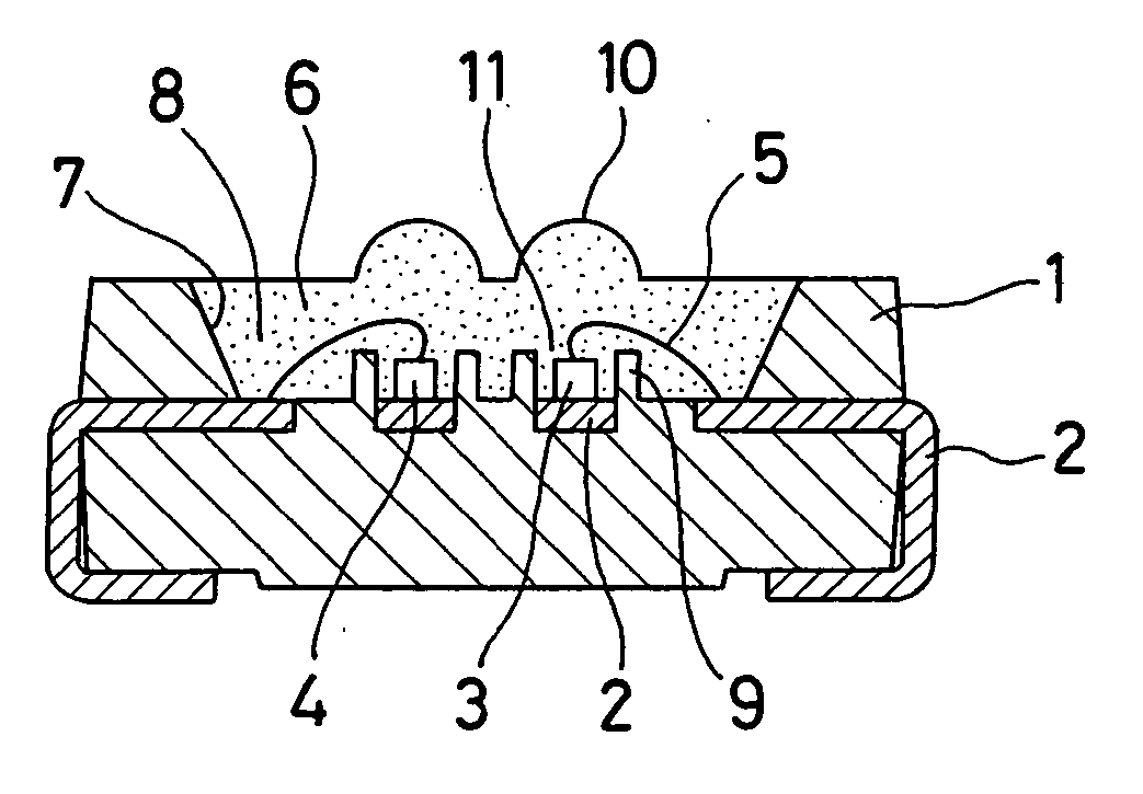
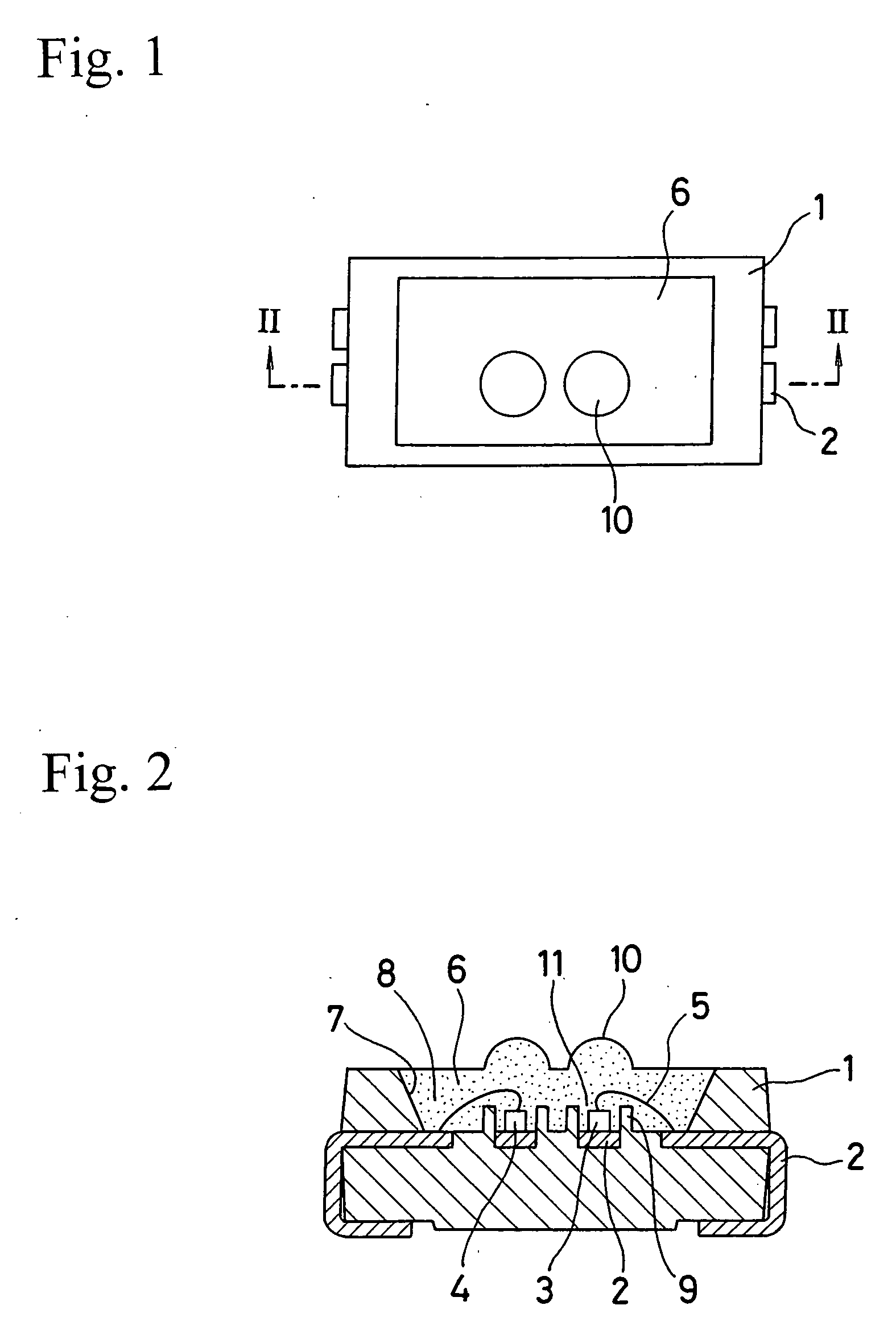
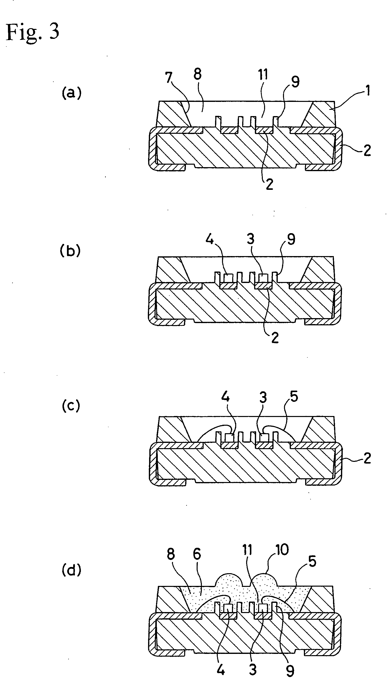
[0051]FIG. 1 is a top view illustrative of an embodiment of an LED device made in accordance with the principles of the invention. FIG. 2 is a cross-sectional view taken along line II-II of FIG. 1. This embodiment is directed to an LED device of the so-called surface-mount type, which includes a reflector 1, a lead frame 2, a red LED chip 3, a green LED chip 4, a bonding wire 5, and a light transmissive resin 6.

[0052] The LED device including these elements can also include the following structure. Plural separate lead frames 2 can be insert-molded in the reflector 1 composed of a white resin having high reflectivity to for...


PUM


Abstract

A plurality of separate lead frames can be insert-molded in a reflector composed of a white resin having a high reflectivity to form a package for an LED device. A cavity is formed in the reflector. The cavity can have an inner circumferential surface that opens wider in an upward direction. Cups can be located in the cavity. Each cup has an outer wall that can be in the form of a cylinder with the bottom formed of each of two separate lead frames. A red LED chip and a green LED chip can be adhesively fixed to the lead frames located on the bottoms of the respective cups. The LED chips can have lower electrodes, which are electrically brought into conduction with the lead frames one by one. The LED chips can also have upper electrodes, which are electrically brought into conduction with the lead frames one by one via bonding wires. A light transmissive resin can be filled in the cavity.

Description

[0001] This application claims the priority benefit under 35 U.S.C. §119 of Japanese Patent Application No. 2004-277764 filed on Sep. 24, 2004, which is hereby incorporated in its entirety by reference. BACKGROUND OF THE INVENTION [0002] 1. Field of the Invention [0003] The invention relates to a light emitting diode (LED) device. More particularly, it relates to an LED device including LED chips of two or more types having different light source colors that are combined as light sources to provide a light of a desired tone by mixing the light emitted from the various LED chips. [0004] 2. Description of the Related Art [0005] A spectrum of light emitted from an LED chip has a sharp rise and fall, which provides a light source color of a tone approximately corresponding to a peak emission wavelength in a spectral distribution. An LED light source having such an optical property may be employed in a method to provide a light of a tone different from the light source color. In this met...

Claims


Application Information

Patent Timeline
Patent Type & Authority Applications(United States)
IPC IPC(8): H01L33/00H01L23/495H01L33/54H01L33/56H01L33/60H01L33/62
CPCH01L25/0753H01L33/486H01L33/60H01L33/62H01L2924/1815H01L2224/48247H01L2224/48091H01L2924/00014
Inventor HANYA, AKIHIKO
Owner STANLEY ELECTRIC CO LTD
Learn More