Decoupling capacitor for an integrated circuit and method of manufacturing thereof

a technology of integrated circuits and capacitors, which is applied in the direction of feed-through capacitors, fixed capacitor details, semiconductor/solid-state device details, etc., can solve the problems of reduced manufacturing throughput, high price, and unsatisfactory use of decoupling capacitors, and achieves better supply voltage stability, reduced manufacturing throughput, and greater effective capacitance

Inactive Publication Date: 2006-03-30
SILICON BANDWIDTH
View PDF4 Cites 24 Cited by
  • Summary
  • Abstract
  • Description
  • Claims
  • Application Information

AI Technical Summary

Benefits of technology

[0009] The present invention relates to a platform that incorporates decoupling capacitors between an IC chip on one hand and a circuit board on the other hand. For example, decoupling capacitors may be provided in a semiconductor die package, thereby providing a decoupling capacitance between the an IC chip housed within the package and a printed circuit board on which the package is mounted. The decoupling capacitors are provided near the IC chip, yielding a lower inductive path and/or greater effective capacitance that helps to stabilize the supply voltage. This platform can enable, among other things, better supply voltage stability because the charge stored in the decoupling capacitors can offset variations. In particular, the present invention provides nove...

Problems solved by technology

The decoupling capacitors are useful from an electrical standpoint, but are far from ideal.
In addition, the placement of the capacitors slows manufacture, leading to reduced manufacturing throughput and higher prices.
Furthermore, the distance between the decoupling capacito...

Method used


Image

  • Decoupling capacitor for an integrated circuit and method of manufacturing thereof
  • Decoupling capacitor for an integrated circuit and method of manufacturing thereof
  • Decoupling capacitor for an integrated circuit and method of manufacturing thereof

Examples


Embodiment Construction

)

[0096] Reference will now be made in detail to the present exemplary embodiment(s) of the invention illustrated in the accompanying drawings. Wherever possible, the same reference numbers will be used throughout the drawings to refer to the same or like parts.

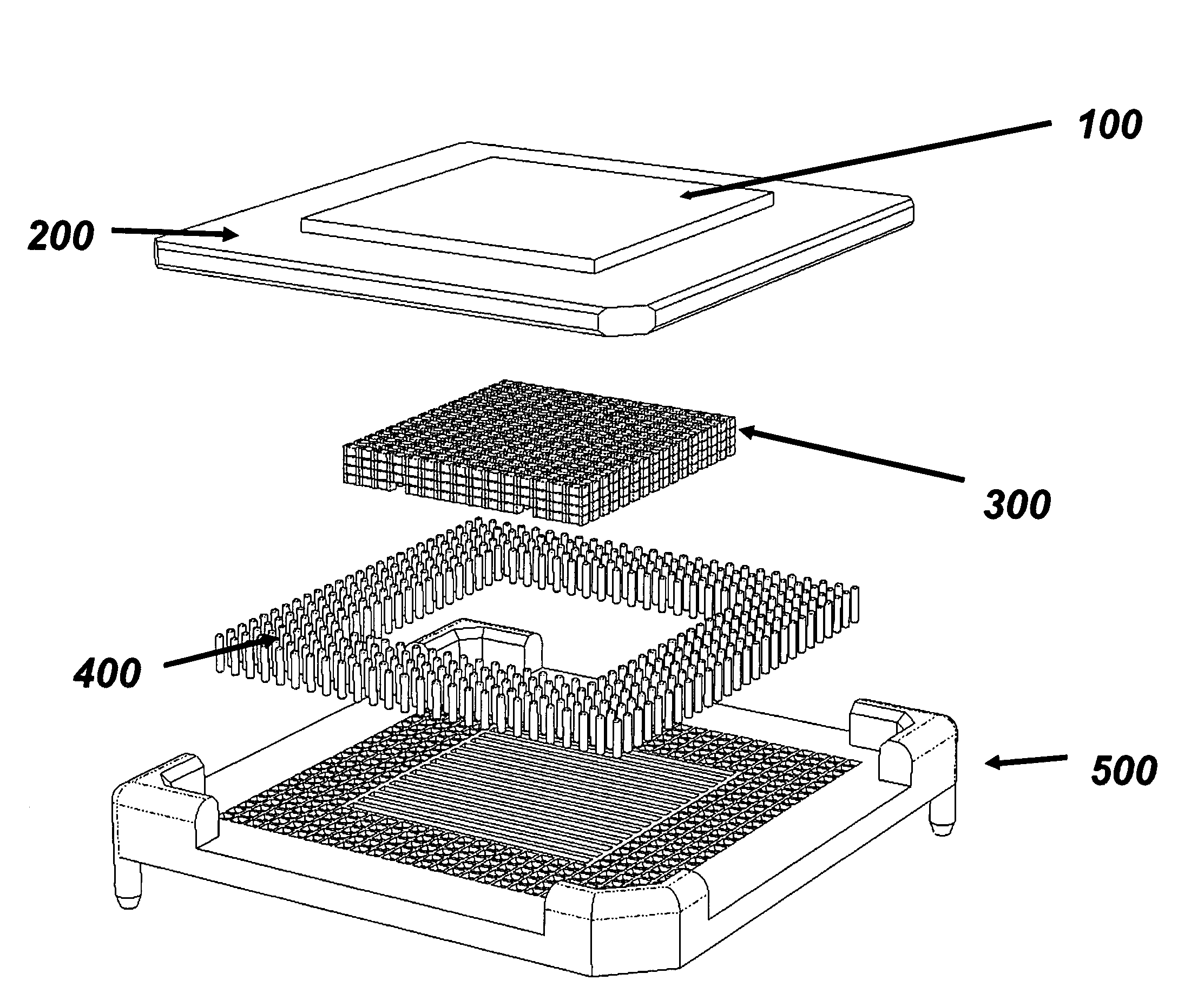
[0097]FIG. 3 illustrates an exploded view of a first exemplary embodiment of a device arrangement 10. The arrangement includes an IC chip or die 100, substrate 200, decoupling capacitor block 300, electrically-conductive pins 400, and main body 500. Chip 100 may include semiconductor devices and circuitry embodying, for example, a microprocessor, microcomputer, application specific integrated circuit, digital signal processor, or other IC. Chip 100 mounts to substrate 200 and makes electrical connection thereto using, for example, bumps, a bumpless interface, tape automated bonding, jumpers, or wire bonds. While FIG. 3 illustrates a single chip 100, it should be appreciated that main body 500 may house multiple chips 100.

[00...


PUM

PropertyMeasurementUnit
Electrical conductivityaaaaaaaaaa
Electrical conductoraaaaaaaaaa

Abstract

A capacitor structure may be incorporated into an interposer or substrate associated with an IC chip to stabilize the input/output signals, such as power and ground, between the IC chip and a printed circuit board. In accordance with one embodiment, the capacitor structure may include a plurality of individual capacitors connected together to form a monolithic capacitor blade having a length, width, and height, wherein each of the length and height of the blade spans multiple of the individual capacitors. The blade includes multiple electrical conductive paths extending the height of the capacitor blade. According to another embodiment, the capacitor structure includes multiple interleaved power and ground layers separated by insulating layers. The power layers connect to power leads and the ground layers connect to ground leads.

Description

FIELD OF THE INVENTION [0001] The present invention relates to voltage supply stabilization and, in particular, to a decoupling capacitor arrangement, to integrated circuit devices that incorporate the decoupling capacitor arrangement, and to methods of manufacturing the foregoing. BACKGROUND OF THE INVENTION [0002] Integrated circuits or “ICs” are the electronic components that run computers, cell phones, and other equipment. ICs are usually mounted on printed circuit boards (PCBs) housed within the equipment. The PCBs have conductive traces that electrically connect together the ICs and permit connection to other components, such as displays, keyboards, speakers, microphones, etc. The ICs are often the electronic elements that control device operation. [0003] ICs are characterized by their operating speed, which is often indicated using their clock rate. For example, computers may be advertised as having a 500 MHz Intel Pentium III microprocessor. The “500 MHz” designation indicat...

Claims


Application Information

Patent Timeline
IPC IPC(8): H01G4/228
CPCH01G4/232H01G4/35H01L23/50H01L2924/01078H01L2924/01079H01L2924/15311Y10T29/49139H05K7/1092H01L2224/16225H01L2224/16235Y10T29/49128Y10T29/43H01L2924/3025H01L2224/0554H01L2224/0557H01L2224/05571H01L2224/05573H01L2924/00014H01L2224/05599H01L2224/0555H01L2224/0556
Inventor CRANE, STANFORD W. JR.HORVATH, ZSOLTNICKEL, JOSHJEON, MYOUNG-SOOOGATA, CHARLEYALCARIA, VINCENTCODD, PATRICK
Owner SILICON BANDWIDTH
Why Eureka
Try Eureka