Method of patterning a substrate by feeding mask defect data forward for subsequent correction

Inactive Publication Date: 2006-03-30
IBM CORP
View PDF0 Cites 3 Cited by
  • Summary
  • Abstract
  • Description
  • Claims
  • Application Information

AI Technical Summary

Problems solved by technology

In photomasks (“masks”) used to pattern features of microelectronic substrates (e.g., transistors, micro-electromechanical (“MEMS”) devices, and other small devices), it is becoming increasingly difficult to meet this requirement.
The costs and amount of time required to fabricate a mask, as well as the number of masks in a set of masks are increasing dramatically, particularly in advanced semiconductor technologies.
The layouts to be patterned by a mask are becoming increasingly complex, containing ever greater numbers of features, while the sizes of such features (e.g., the widths and lengths of lines) shrink with a ground rule that is reduced with succeeding generations of technology.
Unfortunately, it is increasingly difficult to produce photomasks to the requirements of increased complexity and reduced ground rule, such that many photomasks are defective as fabricated.
However, since the repair of masks and the manufacture of new masks require expenditures of both time and money, efforts to address such defects can be costly at the introduction of a new product and can even sometimes hinder its entry into the market.

Method used


Image

  • Method of patterning a substrate by feeding mask defect data forward for subsequent correction
  • Method of patterning a substrate by feeding mask defect data forward for subsequent correction
  • Method of patterning a substrate by feeding mask defect data forward for subsequent correction

Examples


Embodiment Construction

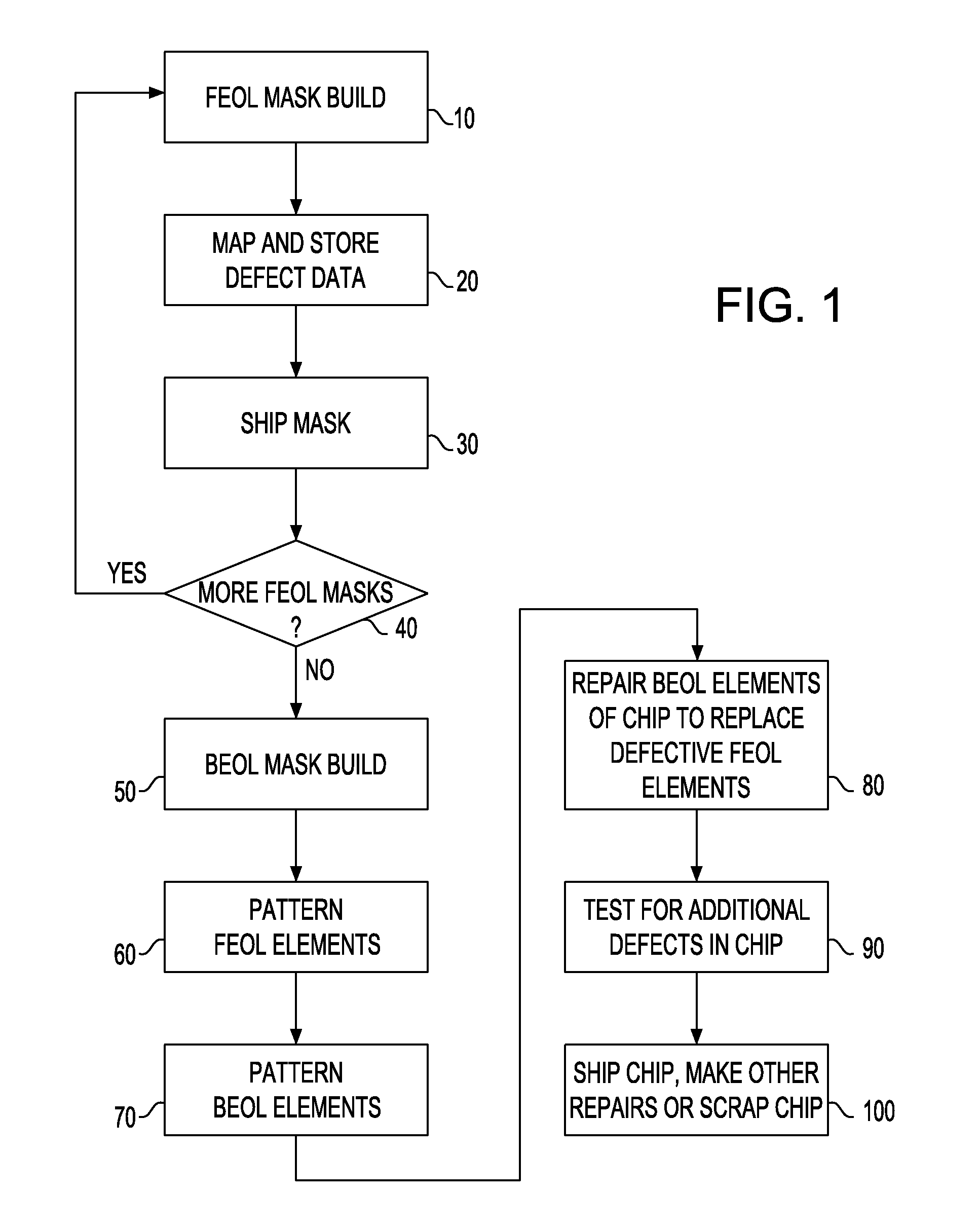
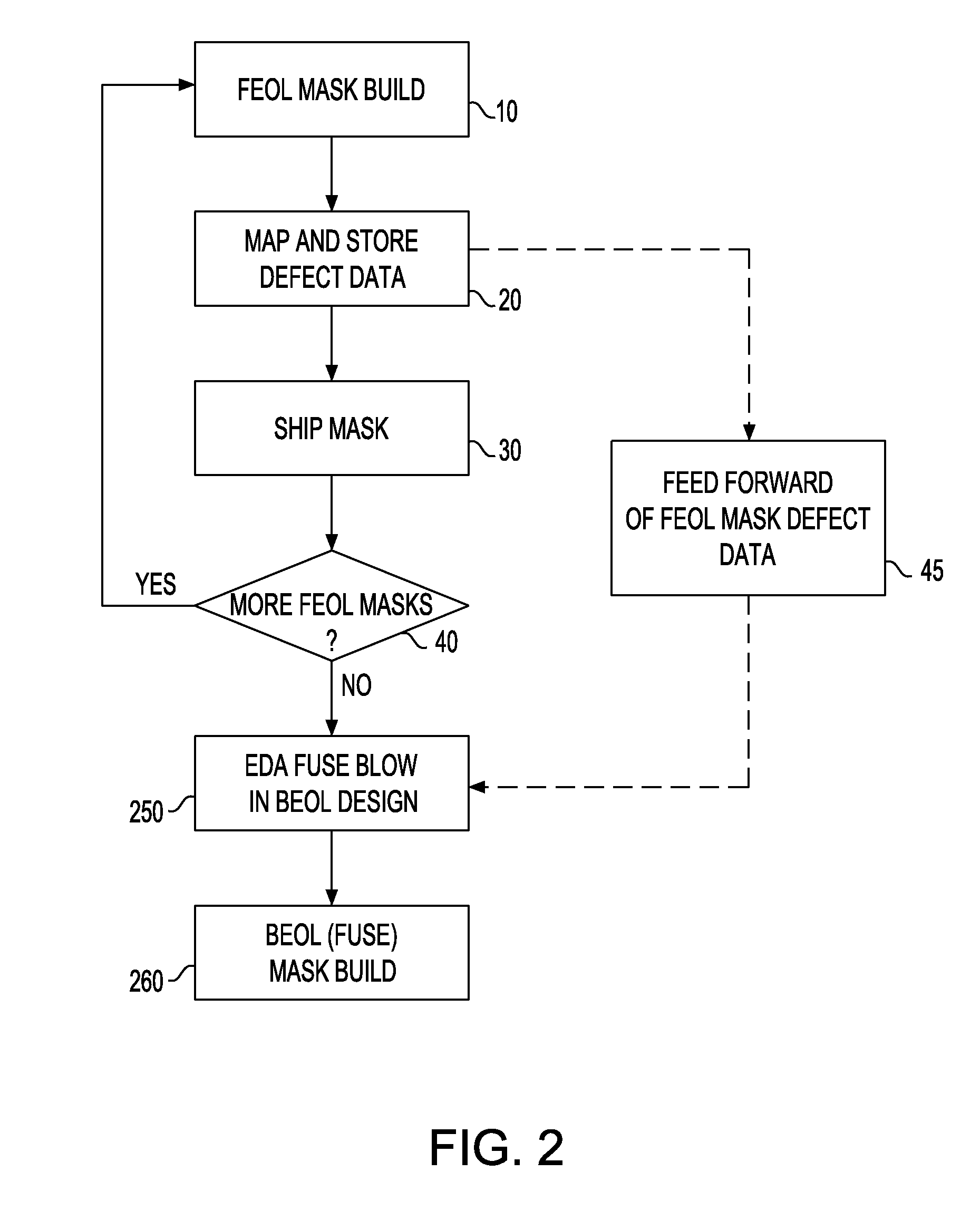
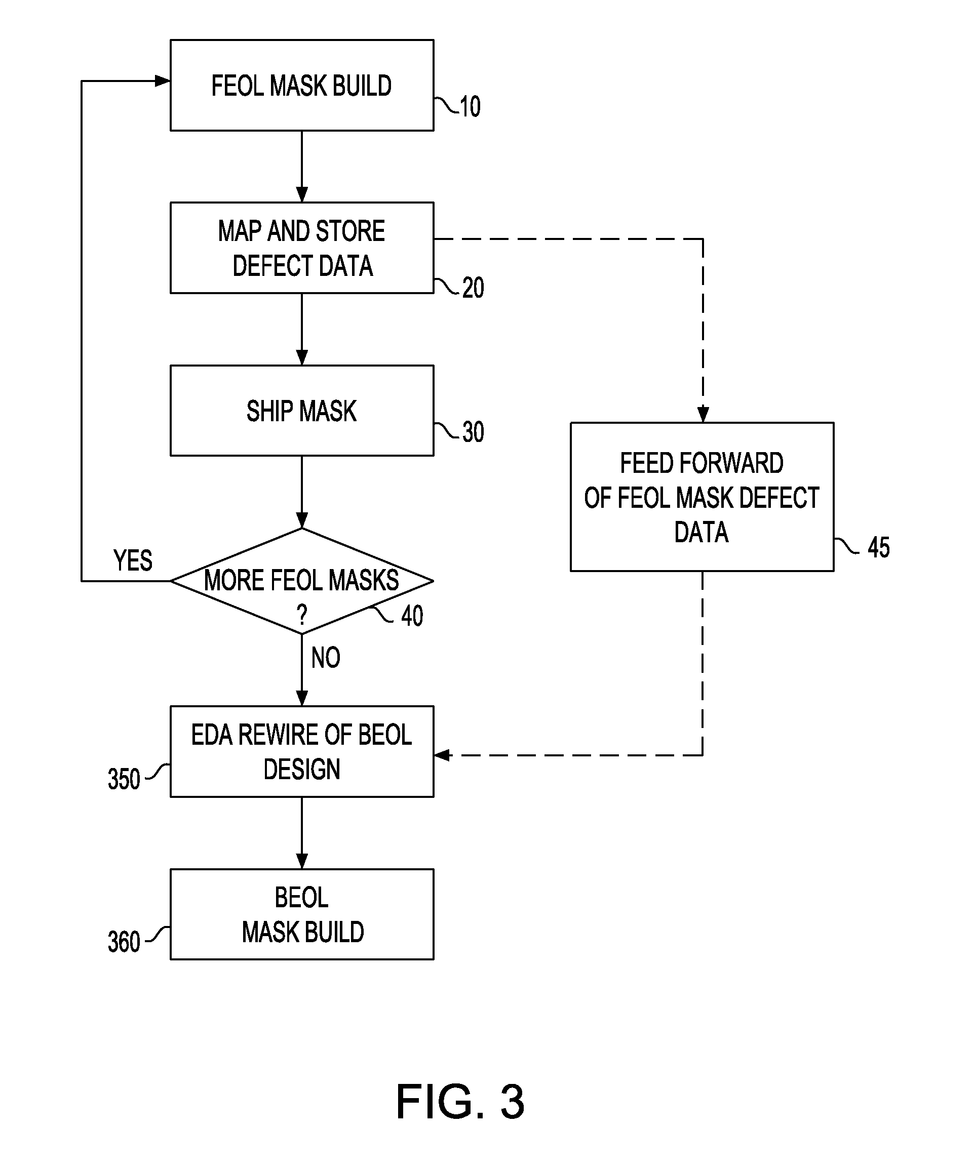
[0010] In view of the difficulties of fabricating masks which are free of defects, a way is provided according to an embodiment of the invention to pattern features of a microelectronic or micro-electromechanical substrate, for example, a chip, integrated circuit or wafer, without requiring masks to be free of defects. Particularly when one mask of a sequential series of masks is found to have a defect, a way is provided to pattern features of a substrate using the defective mask and one or more subsequent sequential masks in the series so as to produce a fully functional substrate which is free of defects.

[0011] For example, in one embodiment, a first mask is checked after fabrication to detect features that are defective. If the mask has no defects, it will be employed as usual to pattern the features of the substrate. However, when the mask is defective, it is not automatically scrapped, as it would be in a conventional process. Instead, the mask will still be used to pattern fe...


PUM


Abstract

A method is provided for patterning a substrate. In such method a first mask, for example, a front-end-of-line (“FEOL”) mask is fabricated, the first mask including a plurality of first features such as FEOL features which are usable to pattern regular elements and redundancy elements of a substrate such as a microelectronic substrate and / or a micro-electromechanical substrate. The first mask is tested, i.e., inspected for defects in the features. Thereafter, a second sequentially used mask, for example, a back-end-of-line (“BEOL”) mask is fabricated which includes a plurality of second features, e.g., BEOL features, such features being usable to pattern a plurality of interconnections between individual ones of the regular elements and between the regular elements and the redundancy elements. The regular elements and the redundancy elements are patterned using the first mask and the interconnections between them are patterned using the second mask. As a result, the interconnections are patterned in a way that corrects for the detected defects in the first mask.

Description

BACKGROUND OF THE INVENTION [0001] The present invention relates to the fabrication of microelectronic and micro-electromechanical devices. [0002] Photomasks used in the fabrication of microelectronic and micro-electromechanical devices, e.g., integrated circuits (“chips”), wafers, and substrates used to interconnect chips typically are required to be free of defects. In photomasks (“masks”) used to pattern features of microelectronic substrates (e.g., transistors, micro-electromechanical (“MEMS”) devices, and other small devices), it is becoming increasingly difficult to meet this requirement. The costs and amount of time required to fabricate a mask, as well as the number of masks in a set of masks are increasing dramatically, particularly in advanced semiconductor technologies. The layouts to be patterned by a mask are becoming increasingly complex, containing ever greater numbers of features, while the sizes of such features (e.g., the widths and lengths of lines) shrink with a ...

Claims


Application Information

Patent Timeline
IPC IPC(8): G03F1/00G06F17/50G03C5/00
CPCG03F1/144G03F7/70466G03F1/72G03F1/70
Inventor RANKIN, JED H.WATTS, ANDREW J.
Owner IBM CORP
Why Eureka
Try Eureka