Method of forming via hole in resin layer

Inactive Publication Date: 2006-03-30
SHINKO ELECTRIC IND CO LTD
View PDF13 Cites 8 Cited by
  • Summary
  • Abstract
  • Description
  • Claims
  • Application Information

AI Technical Summary

Benefits of technology

[0014] According to the present invention, when forming a via hole by firing a laser beam at a resin layer, by dividing the laser beam firing step into a first laser beam firing step for firing a laser beam of the infrared region and a second laser beam firing step for firing a laser beam of the ultraviolet region, even if the resin layer contains inorganic filler with a band gap of 3 to 4 eV, it becomes possible to reliably form a via hole in a short time. Therefore, the remarkable effect is exhibited that it is possible to suitably utilize this when producing a multilayer circuit board provided with an insulating layer having a specific function.BRIEF DESCRIPTION OF DRAWINGS

Problems solved by technology

However, a low dielectric constant and low dielectric loss tangent resin has the problem of difficult removal of the residue produced at the time of laser processing by desmearing.
A board formed using a resin material containing an inorganic filler with a band gap of 3 to 4 eV has the problem that it cannot be effectively formed with a via hole simply by the method of firing a laser beam using a CO2 laser or UV-YAG laser and therefore suffers from unreliable electrical conduction at the via part and the problem that the processing for forming a via hole takes a long time and therefore the method cannot be employed for producing actual products.

Method used


Image

  • Method of forming via hole in resin layer
  • Method of forming via hole in resin layer
  • Method of forming via hole in resin layer

Examples


example 1

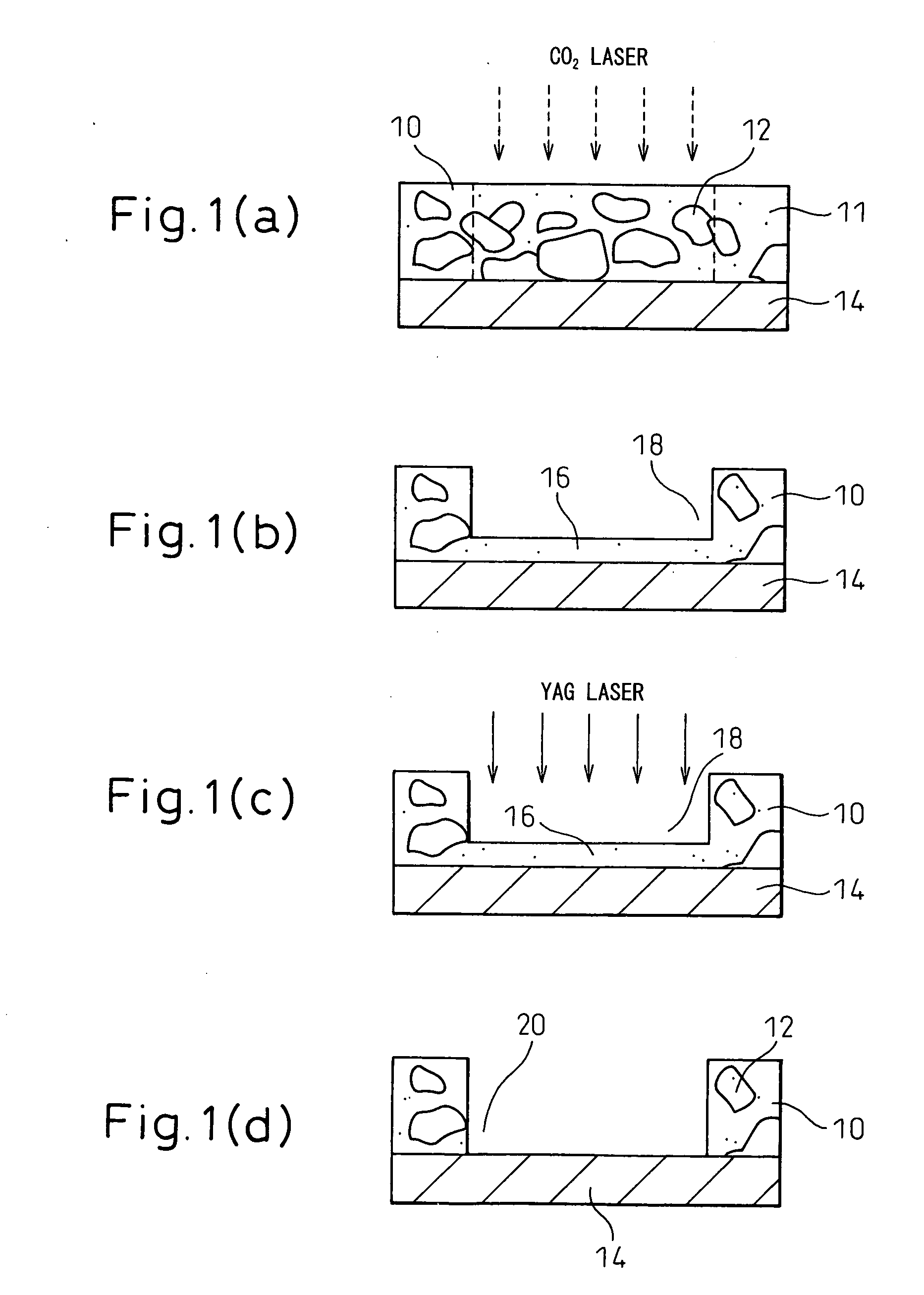
[0031]FIG. 1(a) to FIG. 1(d) are explanatory views of a method of forming a via hole in a resin layer by the method of the present invention (Example 1). Reference numeral 10 is a resin layer, while 14 is an underlying layer. The resin layer 10 includes an inorganic filler 12, so in Example 1, a via hole is formed in a resin layer 10 including titanium oxide as an inorganic filler 12 with a band gap of 3 to 4 eV. As the resin 11 forming the resin layer 10, a polyphenylene ether (PPE) resin was used. The PPE resin is a resin difficult to remove by desmearing, while the inorganic filler 12 is mixed in by a weight ratio with the resin 11 of 1:1. Note that the rate of mixture of the inorganic filler in the present invention is not limited to the rate in Example 1.

[0032] In Example 1 as well, a laser beam is fired at the resin layer in the same way as the conventional method (Comparative Examples 1 to 3) to remove the resin at the location for forming the via hole. In Example 1, the ope...

example 2

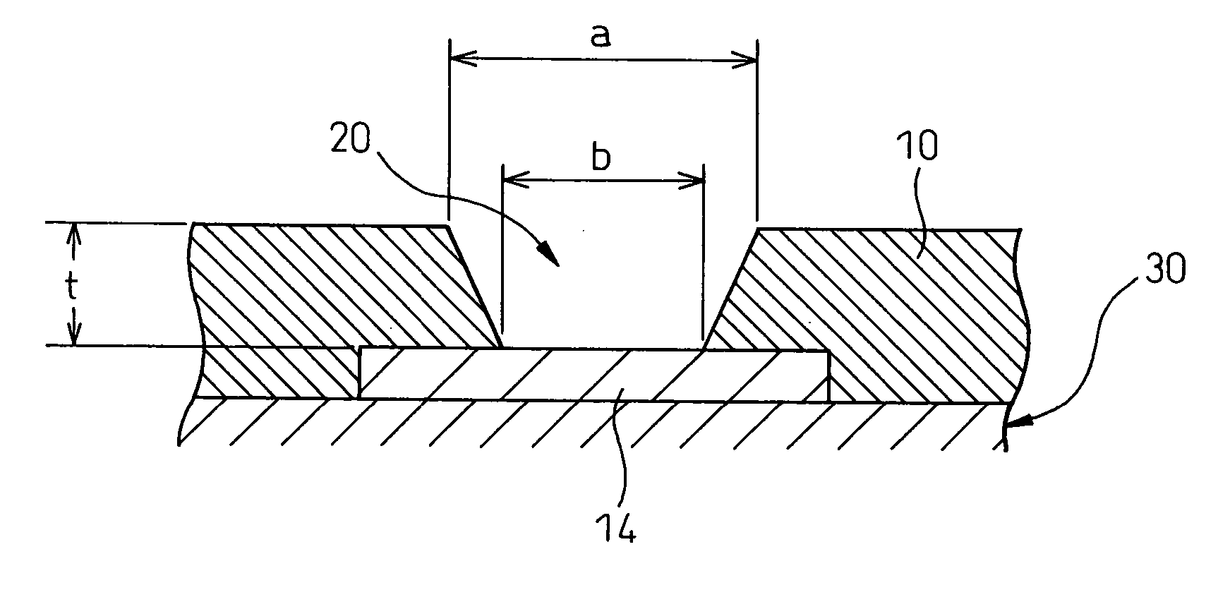
[0041] The diameter of the via hole 20 to be formed in the above Example 1 was changed. That is, in FIG. 4 showing the diameter of the via hole, in Example 1, the diameter a of the via hole 20 was made 90 μm and the diameter b of the bottom was made 60 μm (same in Comparative Examples 1 and 2, Reference Example, and later explained Example 3), while in Example 2, the diameter a of the top of the via hole 20 was made 150 μm and the diameter b of the bottom was made 120 μm. Along with this, for the firing condition of the laser beam fired, in particular the amount fired, the first laser comprised of the CO2 laser fired a 1.0 mJ laser pulse four times per via hole for a total of 4.0 mJ. On the other hand, the second laser comprised of the UV-YAG laser had a wavelength of 355 nm or the same as Example 1, but fired 0.6 mJ per via hole.

[0042] The rest of the conditions are exactly the same as in Example 1.

example 3

[0043] In Example 3, the diameter of the via hole 20 to be formed is the same as Example 1, but the UV-YAG laser used as the second laser is not one having a wavelength 355 nm used in Examples 1 and 2, but one having a wavelength of 266 nm.

[0044] The rest of the conditions are exactly the same as in Example 1.


PUM


Abstract

To reliably expose an underlying layer at a bottom surface of a via hole to form a via hole even at a resin layer including an inorganic filler. A method of forming a via hole by firing a laser beam at a resin layer (10) including an inorganic filler (12) characterized by including a first laser beam firing step of firing a (CO2) laser beam of the infrared region at a position of said resin layer for forming a via hole so as to expel the resin (11) and said inorganic filler (12) and thereby form a hole (18) in the resin layer and a second laser beam firing step of firing a (UV-YAG) laser beam of the ultraviolet region focused at a position where the hole is formed to remove a modified layer (16) of the resin remaining at the bottom of the hole and form a via hole (20) with an underlying layer (14) exposed at its bottom.

Description

TECHNICAL FIELD [0001] The present invention relates to a method of forming a via hole in a resin layer able to be applied when forming a via hole in a resin layer of a multilayer circuit board. BACKGROUND ART [0002] A multilayer circuit board is formed by stacking interconnect patterns through epoxy resins or other resin layers having electrical insulating characteristics. By providing vias so as to pass through the resin layers in the thickness direction, layers of the interconnect patterns are electrically connected. There are several methods for forming a via, but the general practice is to laminate an uncured epoxy resin or other resin film to form a resin layer, fire a CO2 laser beam or UV-YAG laser beam at the resin layer to form a via hole so that the underlying layer of an interconnect pattern is exposed at the bottom surface, then plate the inside surface of the via hole to form a conductive layer electrically connected with the interconnect pattern exposed at the bottom s...

Claims


Application Information

Patent Timeline
IPC IPC(8): H01L21/4763H05K3/00
CPCH05K3/0035H05K2203/108H05K2201/0209H05K3/40
Inventor KOBAYASHI, KAZUTAKA
Owner SHINKO ELECTRIC IND CO LTD
Why Eureka
Try Eureka