
Methods and computer program products for debugging clock-related scan testing failures of integrated circuits

a technology of integrated circuits and scan tests, applied in the field of integrated circuit scan testing, can solve problems such as bad scan path, and achieve the effects of reducing the time to debug scan test failures, reducing integrated chip production costs, and facilitating inspection

Inactive Publication Date: 2006-03-30
AVAGO TECH WIRELESS IP SINGAPORE PTE
View PDF9 Cites 9 Cited by
  • Summary
  • Abstract
  • Description
  • Claims
  • Application Information

AI Technical Summary

Benefits of technology

[0016] The invention reduces the time to debug scan test failures, which reduces integrated chip production costs and streamlines integrated circuit manufacturing.

Problems solved by technology

A scan path is bad if it is not producing any output.

Method used


Image

  • Methods and computer program products for debugging clock-related scan testing failures of integrated circuits
  • Methods and computer program products for debugging clock-related scan testing failures of integrated circuits
  • Methods and computer program products for debugging clock-related scan testing failures of integrated circuits

Examples


Embodiment Construction

[0023] While the present invention is described herein with reference to illustrative embodiments for particular applications, it should be understood that the invention is not limited thereto. Those skilled in the art with access to the teachings provided herein will recognize additional modifications, applications, and embodiments within the scope thereof and additional fields in which the invention would be of utility.

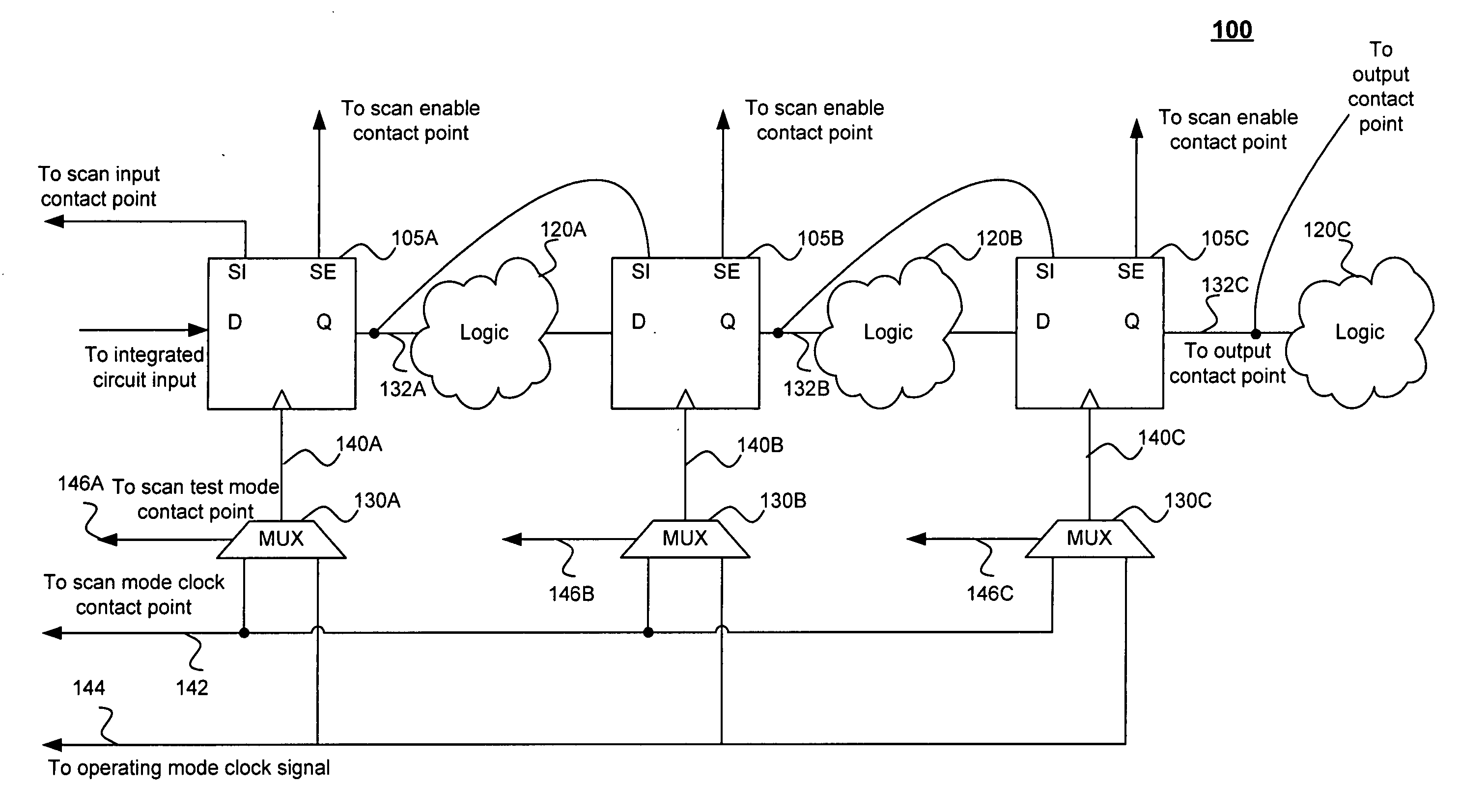
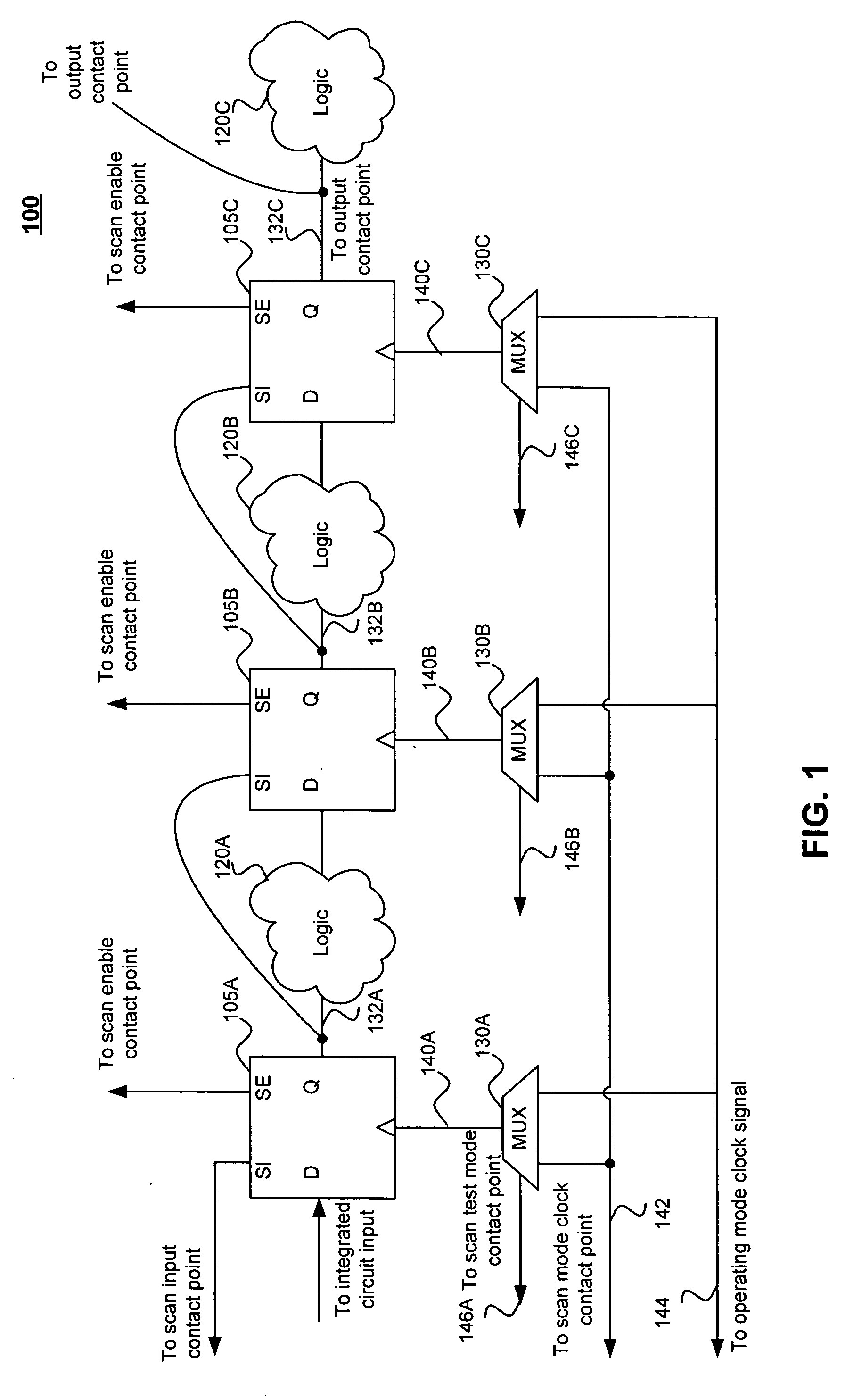
[0024]FIG. 1 illustrates an example of a truncated scan path within an integrated circuit. The scan path includes flip-flop 105A, flip-flop 105B, and flip-flop 105C. Flip-flop 105A represents the first flip-flop in the scan path. An SI input on flip-flop 105A is coupled to a scan input contact point. The scan input contact point provides an interface to an automated testing unit that allows test patterns to be inputted. An SE input on flip-flop 105A is coupled to a scan enable contact point.

[0025] Two modes exist within scan testing: shift mode and capture mode. I...


PUM


Abstract

The present invention is directed to a method for debugging scan testing failures of integrated circuits. The method includes identifying good and bad scan paths among a set of scan paths. A scan path is bad if it is not producing any output. A scan path is good if it is producing a correct output. A clock set is generated for each scan path. The clock set includes all clock elements whose outputs impact the scan path. A union of the scan path clock sets for the bad scan paths is created. Good clock elements are removed from the union. A clock element is presumed to be good if it is associated with a good scan path. Clock elements remaining within the union of clock sets for the bad scan paths are analyzed to determine the source of errors. In one embodiment, multiple input clock elements in all bad scan paths are analyzed first, followed by analysis of single input clock elements in all bad scan paths and followed by analysis of any other clock elements in any of the bad scan paths. In an alternative embodiment, failure probabilities are associated with clock elements to prioritize analysis and debugging.

Description

BACKGROUND OF THE INVENTION [0001] 1. Field of the Invention [0002] The present invention relates to integrated circuits, and more particularly, to scan testing of integrated circuits. [0003] 2. Background of Invention [0004] Effective testing of integrated circuits significantly enhances the ability of integrated circuit developers and manufacturers to provide reliable devices. Various techniques have been employed to test integrated circuits during the manufacturing process. One such technique that is commonly known, and has been used within the industry for over twenty years is scan testing. [0005] Scan testing provides an efficient approach to testing the structural integrity of devices, such as flip-flops, within a complex integrated circuit. Scan testing does not test integrated circuit-level functionality. Rather, test personnel use scan testing to confirm that individual flip-flops within an integrated circuit function properly. The sheer number of flip-flops within an integ...

Claims


Application Information

Patent Timeline
IPC IPC(8): G01R31/28
CPCG01R31/318536
Inventor GUETTAF, AMAR
Owner AVAGO TECH WIRELESS IP SINGAPORE PTE
Learn More