PRAMs having a plurality of active regions located vertically in sequence and methods of forming the same

a technology of active regions and prams, which is applied in the direction of bulk negative resistance effect devices, electrical devices, semiconductor devices, etc., can solve the problems of low design pattern fidelity of prams, limited photolithography process, and difficulty in rapidly changing phase of phase change layer patterns, etc., to achieve good design performance

Active Publication Date: 2006-04-13
SAMSUNG ELECTRONICS CO LTD
View PDF4 Cites 51 Cited by
  • Summary
  • Abstract
  • Description
  • Claims
  • Application Information

AI Technical Summary

Benefits of technology

[0009] The invention also provides a method of forming a PRAM having a plurality of active regions located vertically in sequence, by which integration of cell and peripheral transistors increases in a cell array region and a peripheral circuit region to exhibit good design performance.

Problems solved by technology

However, the PRAM typically does not have a gate pattern having high design pattern fidelity on the semiconductor substrate due to gradual reduction of a given design rule.
This is because a photolithography process has a limit in defining a pattern image on a photoresist layer corresponding to the reduced design rule.
In addition, the gate pattern in the cell array region has a poor current driving capability compared to that prior to the reduced design rule, such that there is difficulty in rapidly changing the phase of the phase change layer pattern.
However, in the structure and the forming method, if the thicknesses of the first and second insulating layers are too small, source or drain regions of the transistors on the first through third active layers may contact each other.
Accordingly, the transistors may exhibit undesired performance characteristics.

Method used


Image

  • PRAMs having a plurality of active regions located vertically in sequence and methods of forming the same
  • PRAMs having a plurality of active regions located vertically in sequence and methods of forming the same
  • PRAMs having a plurality of active regions located vertically in sequence and methods of forming the same

Examples


Embodiment Construction

[0020] The present invention will now be described more fully hereinafter with reference to the accompanying drawings, in which preferred embodiments of the invention are shown. It will be understood that when a layer is referred to as being “on” other layer or substrate, it can be directly on the other layer or substrate, or intervening layers may also be present. Like numbers refer to like elements throughout.

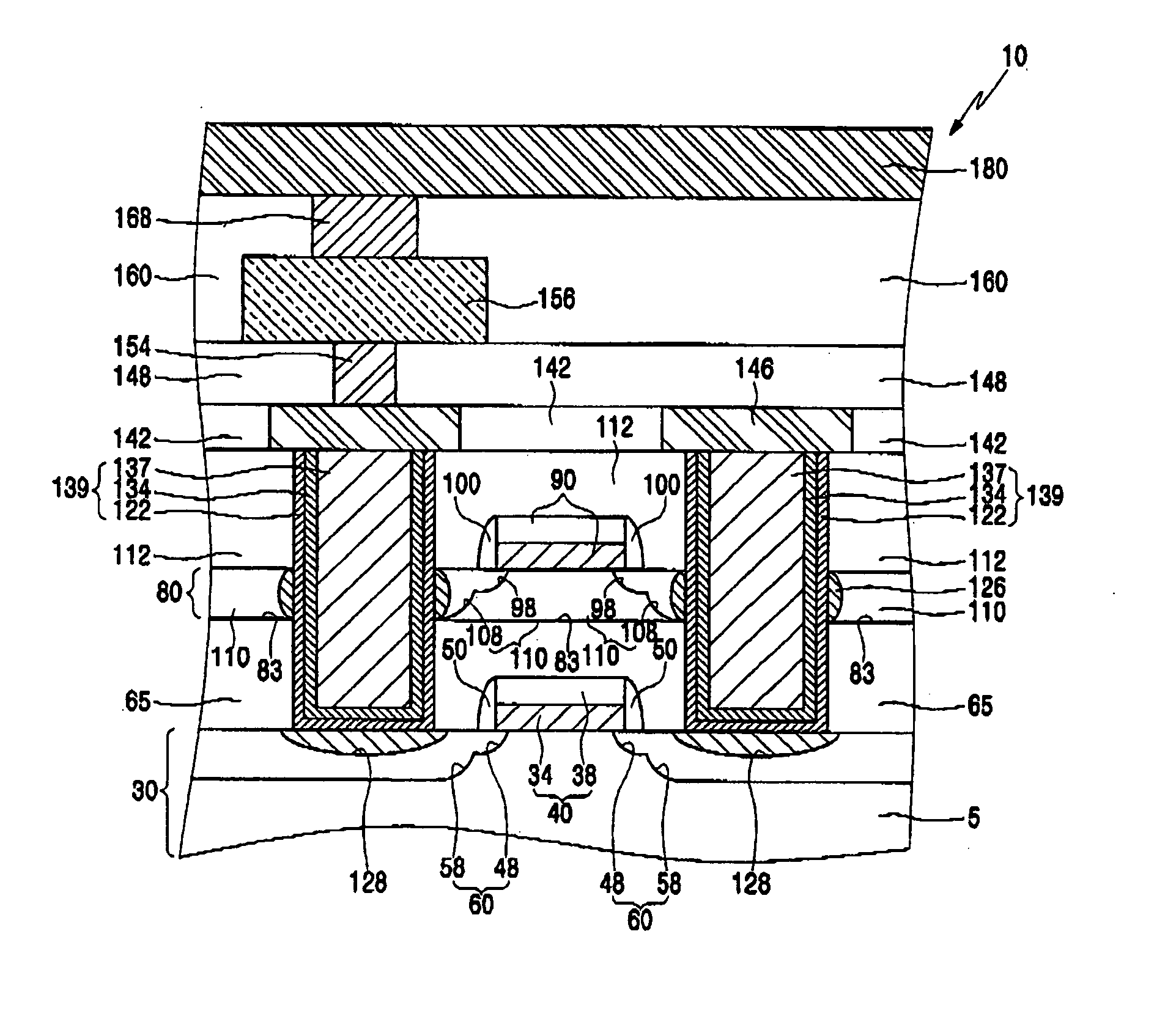
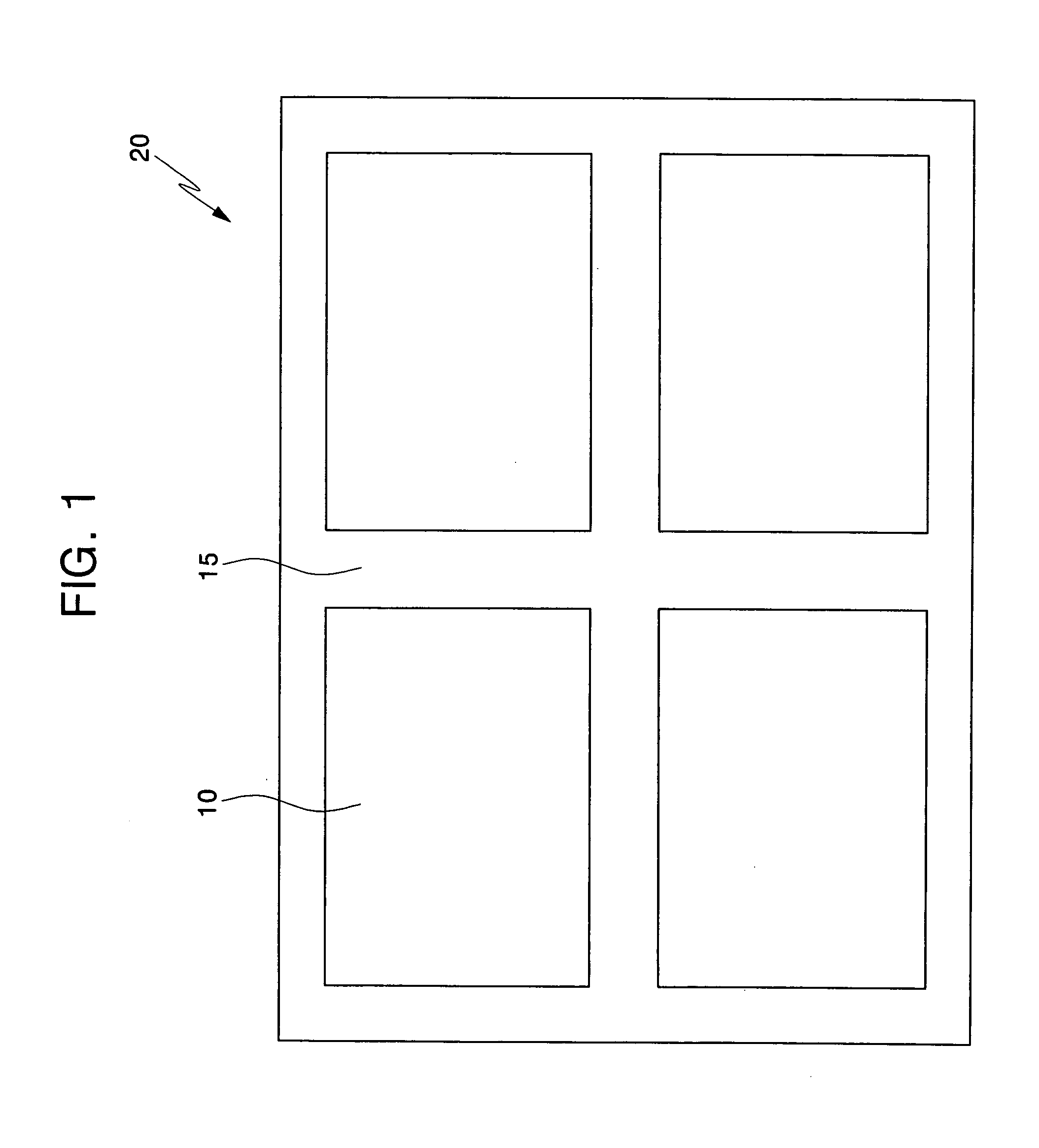
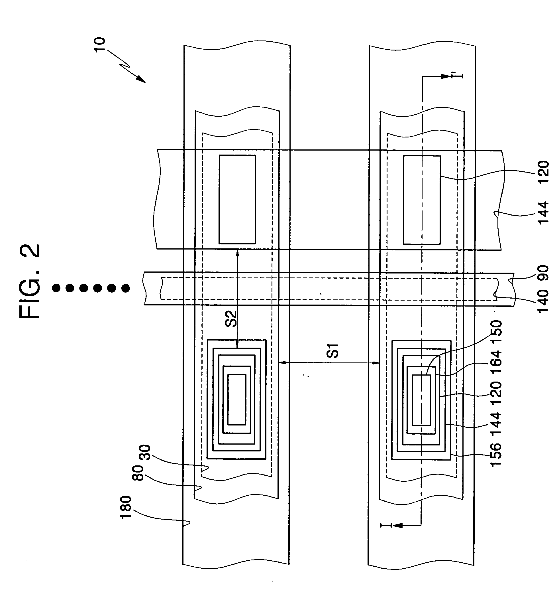
[0021]FIG. 1 is a layout view of a PRAM according to the invention, and FIGS. 2 and 3 are layout views of active regions of a cell array region and a peripheral circuit region of FIG. 1, respectively. Further, FIGS. 4 and 5 are cross-sectional views of the PRAM taken along by lines I-I′ of FIGS. 2 and 3, respectively.

[0022] Referring to FIGS. 1 to 5, a PRAM 20 includes a cell array region 10 and a peripheral circuit region 15 as shown in FIG. 1. The cell array region 10 stores data through a phase change layer pattern 156 as showin in FIG. 4. The peripheral circuit region 1...


PUM


Abstract

There are provided PRAMS having a plurality of active regions located vertically in sequence and methods of forming the same. The PRAM and the method provide an approach to rapidly changing phase in a phase change layer pattern with a given design rule. A semiconductor substrate defining at least one reference active region is prepared in a cell array region and a peripheral circuit region. Other semiconductor substrates on a vertical line passing a main surface of the reference active region are located in sequence. The other semiconductor substrates define other active regions, respectively. A lower cell gate pattern is formed on the semiconductor substrate of the reference active region, and upper cell gate patterns are disposed on the other semiconductor substrates of the other active regions, respectively.

Description

REFERENCE TO PRIORITY APPLICATION [0001] This application claims priority to Korean Application Serial No. 2004-80546, filed Oct. 8, 2004, the contents of which are hereby incorporated herein by reference. FIELD OF THE INVENTION [0002] The invention relates to phase-change random access memories (PRAMs) and methods of forming the same, and more particularly, to PRAMs having a plurality of active regions located vertically in sequence and methods of forming the same. BACKGROUND OF THE INVENTION [0003] Generally, a PRAM has a cell array region and a peripheral circuit region in which semiconductor discrete devices are arranged. The cell array region has gate patterns on a main surface of a semiconductor substrate and phase change layer patterns above the gate patterns. The cell array region has a plug for electrically connecting a gate pattern and a phase change layer pattern in one cell. In the PRAM, a change of phase of the crystal structure of the phase change layer pattern is init...

Claims


Application Information

Patent Timeline
Patent Type & Authority Applications(United States)
IPC IPC(8): H01L29/02
CPCH01L27/2436H01L45/06H01L45/144H10B63/30H10N70/231H10N70/8828H10N70/821
Inventor PARK, JAE-HYUNAN, HYEONG-GEUNAHN, SU-JINSONG, YOON-JONGYOUN, HYUNG-JOOKIM, KYU-CHUL
Owner SAMSUNG ELECTRONICS CO LTD
Why Eureka
Try Eureka