Method for depositing nanolaminate thin films on sensitive surfaces

a technology of nanolaminate and sensitive surfaces, applied in the field of thin films, can solve problems such as introducing many new problems

Inactive Publication Date: 2006-04-13
ASM INTERNATIONAL
View PDF41 Cites 62 Cited by
  • Summary
  • Abstract
  • Description
  • Claims
  • Application Information

AI Technical Summary

Problems solved by technology

While ALD has many potential applications to semiconductor fabrication, integrating these new processes into established process flows can introduce many new issues.

Method used


Image

  • Method for depositing nanolaminate thin films on sensitive surfaces
  • Method for depositing nanolaminate thin films on sensitive surfaces
  • Method for depositing nanolaminate thin films on sensitive surfaces

Examples


example 1

The Deposition of TiN from TiCl4 and NH3

[0183] A 200-mm silicon wafer coated with PVD copper was loaded into a Pulsar 2000™ ALD reactor, commercially available from ASM Microchemistry Oy of Espoo, Finland. The substrate was heated to 400° C. in a flowing nitrogen atmosphere. The pressure of the reactor was adjusted to about 5 mbar by the mass flow controller on the nitrogen line and a vacuum pump. Next, a TiNx layer was grown by ALD from sequential pulses of TiCl4 and NH3 that were separated by inert nitrogen gas.

[0184] One deposition cycle consisted of the following steps: [0185] TiCl4 pulse, for 0.05 s [0186] N2 purge for 1.0 s [0187] NH3 pulse for 0.75 s [0188] N2 purge for 1.0 s

[0189] This cycle was repeated 300 times to form about a 5-nm TiNx film. The growth rate of the TiNx film was about 0.17 Å / cycle. Then the wafer was unloaded from the reactor for analysis. Four-point probe and Energy Dispersive Spectroscopy (EDS) measurements gave a resistivity of 150 μΩcm.

6TiCl4(g)+8...

example 2

Deposition of WN from WF6 and NH3

[0192] A 200-mm silicon wafer coated with PVD copper was loaded to a Pulsar 2000 ALD reactor. The substrate was heated to 400° C. in a flowing nitrogen atmosphere. The pressure of the reactor was adjusted to about 5 mbar by the mass flow controller on the nitrogen line and a vacuum pump. Next, a WNx layer was grown by ALD from sequential pulses of WF6 and NH3 that were separated by inert nitrogen gas.

[0193] One deposition cycle consisted of the following steps: [0194] WF6 pulse for 0.25 s [0195] N2 purge for 1.0 s [0196] NH3 pulse for 0.75 s [0197] N2 purge for 1.0 s

[0198] This cycle was repeated 70 times to form about a 5-nm WNx film. The growth rate of the WNx film was about 0.6 Å / cycle. Then the wafer was unloaded from the reactor for analysis.

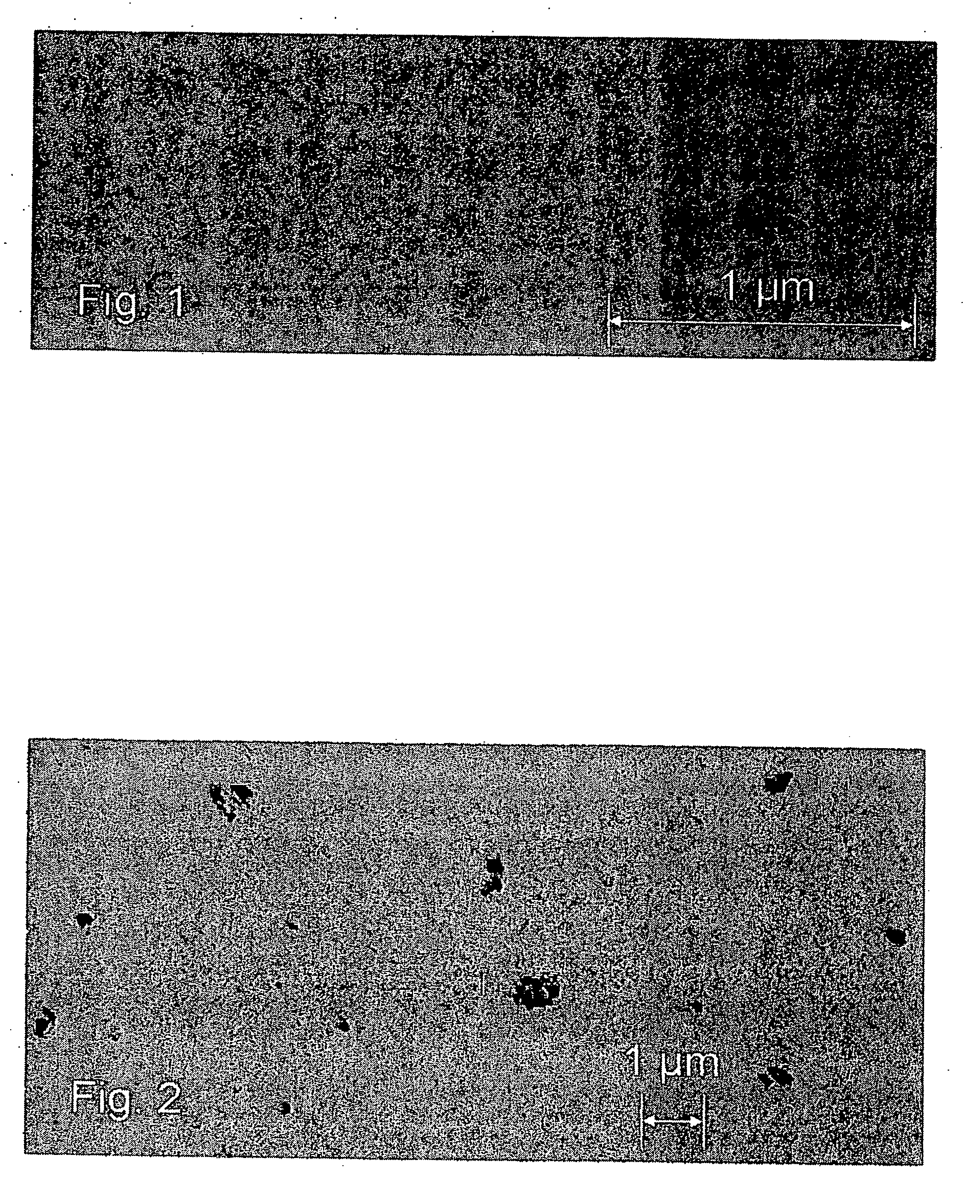
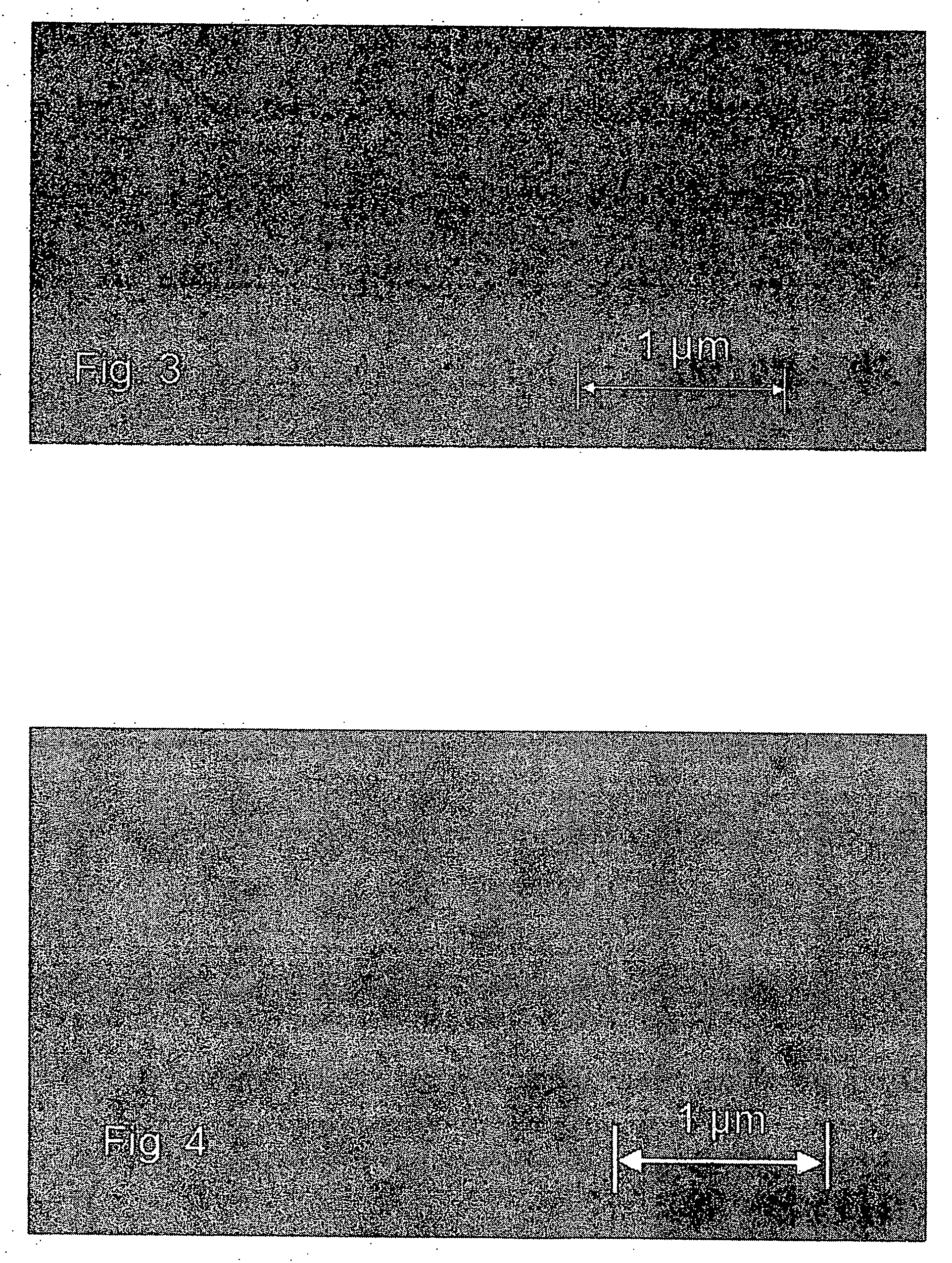
[0199] Etch damage to the copper film was visible even under an optical microscope because of the nitride process. A lot of HF was evolves from the process (R38). HF may attack the copper surface (R39). ...

example 3

Deposition of WCx with a Gettering Compound

[0200] A 200-mm silicon wafer coated with PVD copper was loaded into a Pulsar 2000™ ALD reactor. The substrate was heated to about 400° C. in a flowing nitrogen atmosphere. The pressure of the reactor was adjusted to about 5 mbar by the mass flow controller on the nitrogen line and a vacuum pump. A thin film rich in tungsten metal was grown by ALD from sequential pulses of WF6 and triethyl boron (TEB), which were separated by inert nitrogen gas.

[0201] One deposition cycle consisted of the following steps: [0202] WF6 pulse for 0.25 s [0203] N2 purge for 1.0 s [0204] TEB pulse 0.05 for s [0205] N2 purge for 1.0 s

[0206] This cycle was repeated 70 times to form about a 5-nm W-rich tungsten carbide film. The growth rate of the thin film was about 0.6 Å / cycle. Then the wafer was unloaded from the reactor for analysis. No corrosion of copper was observed by Scanning Electron Microscopy (referred to as SEM hereinafter). The exact reaction mechan...


PUM

PropertyMeasurementUnit
thicknessaaaaaaaaaa
voltageaaaaaaaaaa
thicknessaaaaaaaaaa

Abstract

The present method provides tools for growing conformal metal nitride, metal carbide and metal thin films, and nanolaminate structures incorporating these films, from aggressive chemicals. The amount of corrosive chemical compounds, such as hydrogen halides, is reduced during the deposition of transition metal, transition metal carbide and transition metal nitride thin films on various surfaces, such as metals and oxides. Getter compounds protect surfaces sensitive to hydrogen halides and ammonium halides, such as aluminum, copper, silicon oxide and the layers being deposited, against corrosion. Nanolaminate structures (20) incorporating metal nitrides, such as titanium nitride (30) and tungsten nitride (40), and metal carbides, and methods for forming the same, are also disclosed.

Description

CROSS-REFERENCE TO RELATED APPLICATIONS [0001] The present application is a continuation of U.S. application Ser. No. 10 / 969,297, filed Oct. 19, 2004, which is a divisional of U.S. application Ser. No. 10 / 049,125, filed Aug. 20, 2002, which in turn is the U.S. national phase of PCT application no. PCT / US00 / 28654 filed Oct. 16, 2000, and claims priority under 35 U.S.C. §119 to U.S. provisional application Nos. 60 / 159,799, filed Oct. 15, 1999 and 60 / 176,948, filed Jan. 18, 2000 and Finnish patent application numbers FI19992233, filed Oct. 15, 1999, FI19992234, filed Oct. 15, 1999, FI19992235, filed Oct. 15, 1999, and FI20000564, filed Mar. 10, 2000. Each of the priority applications is here by incorporated by reference.BACKGROUND OF THE INVENTION [0002] 1. Field of the Invention [0003] The present invention relates generally to depositing thin films on substrates by alternated self-saturating chemistries. More particularly, the present invention relates to preventing the corrosion of ...

Claims


Application Information

Patent Timeline
Patent Type & Authority Applications(United States)
IPC IPC(8): H01L21/44C23C16/32C23C16/34C23C16/44C23C16/455C30B25/02C30B29/02C30B29/36C30B29/38H01L21/285H01L21/768
CPCC23C16/32C23C16/34C23C16/44C23C16/4401C23C16/45525C23C16/45529C23C16/45534C30B25/02C30B29/02C30B29/36C30B29/38H01L21/28562H01L21/28568H01L21/76843H01L21/76846H01L21/76877
Inventor ELERS, KAI-ERIKHAUKKA, SUVI P.SAANILA, VILLE ANTEROKAIPIO, SARI JOHANNASOININEN, PEKKA JUHA
Owner ASM INTERNATIONAL
Why Eureka
Try Eureka