Methods for pretreatment of group iii-nitride depositions

a technology of nitride and pretreatment method, which is applied in the direction of semiconductor devices, electrical equipment, basic electric elements, etc., can solve the problems of poor crystal quality, poor etching quality, and the inability to separate substrate etching and alon or alon deposition for better optimization, so as to improve lateral growth, reduce or tune the stress, and reduce the density of threading dislocation

Inactive Publication Date: 2012-11-22
APPLIED MATERIALS INC
View PDF8 Cites 22 Cited by
  • Summary
  • Abstract
  • Description
  • Claims
  • Application Information

AI Technical Summary

Benefits of technology

[0007]Embodiments of the present disclosure relate to methods for pretreatment of substrates or / and group III-nitride layers for manufacturing devices such as light emitting diodes (LEDs), laser diodes (LDs) or power electronic devices. In one embodiment of the present disclosure, a method includes providing one or more substrates having an aluminum containing surface in a processing chamber and exposing a surface of each of the one or more substrates having an aluminum containing surface to a pretreatment gas mixture to form a pretreated surface. In another embodiment, a method of forming a compound nitride structure includes exposing an aluminum containing surface of group III-nitride layers on one or more substrates to a pretreatment gas mixture to form a pretreated surface. In another embodiment, a method of forming a compound nitride structure includes exposing a first pretreated surface of one or more substrates having an aluminum containing surface to a second pretreatment gas mixture to form a second pretreated surface. The pretreatment gas mixtures may include ammonia gas (NH3), an aluminum halide gas (e.g., AlCl3, AlCl), and an etchant containing gas that includes a halogen gas (e.g., Cl2) or hydrogen halide gas (e.g., HCl). The pretreatment procedure could enhance the lateral growth for subsequent group III-nitride deposition, which results in the decrease of threading dislocation density in the subsequently deposited layers. The pretreatment procedure can also reduce or tune the stress in the subsequently deposited layers and final device structures.

Problems solved by technology

It is expected that such a 3D growth leads to rough group III-nitrides surfaces and poor crystal quality.
However, traditional methods for treating aluminum oxide containing substrates cannot separate substrate etching and AlN or AlON deposition for better optimization (e.g., sapphire).
The pretreatment procedure could enhance the lateral growth for subsequent group III-nitride deposition, which results in the decrease of threading dislocation density in the subsequently deposited layers.

Method used


Image

  • Methods for pretreatment of group iii-nitride depositions
  • Methods for pretreatment of group iii-nitride depositions
  • Methods for pretreatment of group iii-nitride depositions

Examples


Embodiment Construction

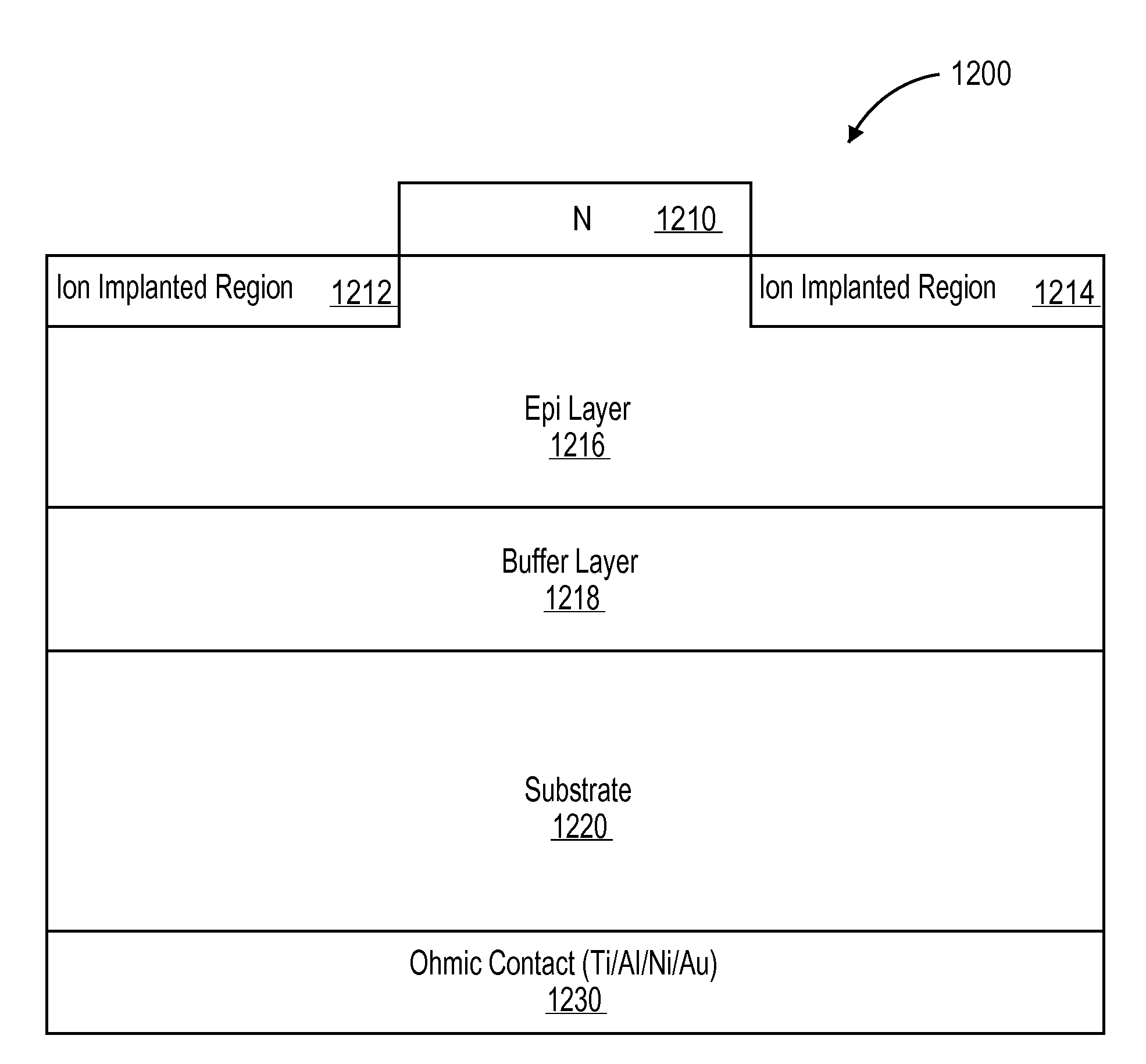
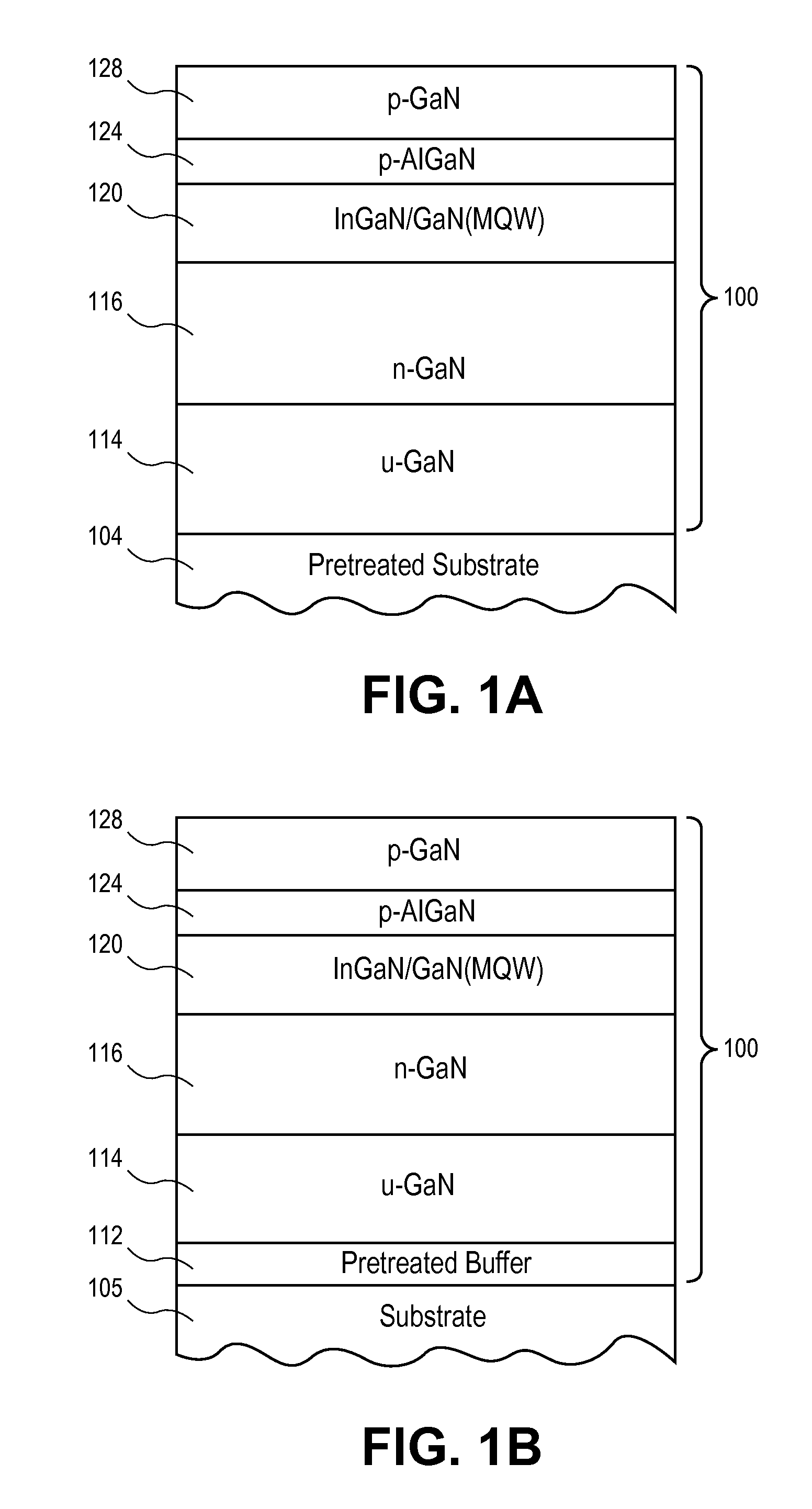
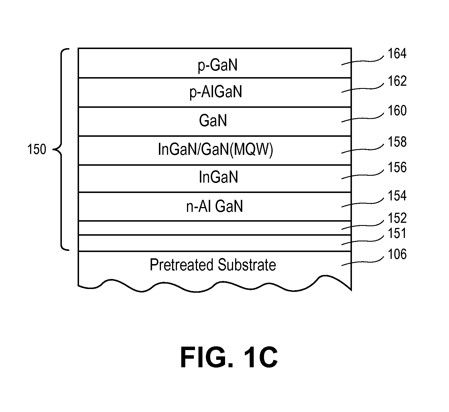
[0021]The present disclosure generally provides methods for manufacturing group III-nitride semiconductor devices. In one embodiment of the present disclosure, a method includes treating a substrate having an aluminum containing surface by exposing the aluminum containing surface to a pretreatment gas mixture that includes ammonia, an etchant containing gas, and an aluminum halide gas. The etchant containing gas includes a halogen gas or hydrogen halide gas. In some embodiments, the etchant containing gas may be selected from the group consisting of chlorine gas (Cl2), bromine gas (Br2), iodine gas (I2), hydrogen chloride gas (HCl), hydrogen bromide gas (HBr), hydrogen iodide gas (HI), combinations thereof, and mixtures thereof. The pretreatment gas mixture reacts with the aluminum containing surface and forms a layer, or a formed region, of aluminum nitride (AlN) and / or aluminum oxynitride (AlON) in case of oxygen containing surface on the substrate (e.g., sapphire). The layer of A...


PUM

PropertyMeasurementUnit
thicknessaaaaaaaaaa
thicknessaaaaaaaaaa
thicknessaaaaaaaaaa

Abstract

Embodiments of the present disclosure relate to methods for pretreatment of substrates and group III-nitride layers for manufacturing devices such as light emitting diodes (LEDs), laser diodes (LDs) or power electronic devices. One embodiment of the present disclosure provides a method including providing one or more substrates having an aluminum containing surface in a processing chamber and exposing a surface of each of the one or more substrates having an aluminum containing surface to a pretreatment gas mixture to form a pretreated surface. The pretreatment gas mixture includes ammonia (NH3), an aluminum halide gas (e.g., AlCl3, AlCl) and an etchant containing gas that includes a halogen gas (e.g., Cl2) or hydrogen halide gas (e.g., HCl).

Description

RELATED APPLICATIONS[0001]This application claims the benefit of Provisional Application No. 61 / 488,673, filed May 20, 2011, which is incorporated herein by reference.FIELD[0002]Embodiments of the present disclosure relate to the manufacture of semiconductor devices. More particularly, embodiments of the present disclosure relate to methods for pretreatment of substrates for manufacturing group III nitride semiconductor devices.DESCRIPTION OF THE RELATED ART[0003]Group III-nitride semiconductors are finding greater importance in the development and fabrication of a variety of semiconductor devices, such as short wavelength light emitting diodes (LEDs), laser diodes (LDs), and electronic devices including high power, high frequency, high temperature transistors and integrated circuits. Light emitting diodes (LEDs) and laser diodes (LDs) are fabricated by depositing group III-nitrides on most commonly used sapphire substrates. Group III-nitrides can be deposited by metal organic chemi...

Claims


Application Information

Patent Timeline
Patent Type & Authority Applications(United States)
IPC IPC(8): H01L21/311
CPCH01L21/0242H01L21/02458H01L33/007H01L21/0262H01L21/02658H01L21/0254
Inventor MELNIK, YURIYCHEN, LUKOJIRI, HIDEHIRO
Owner APPLIED MATERIALS INC
Why Eureka
Try Eureka