Production method for semiconductor substrate and production method for field effect transistor and semiconductor substrate and field effect transistor

a production method and semiconductor technology, applied in the direction of semiconductor devices, electrical devices, basic electric elements, etc., can solve the problems of crystallinity, the surface or interface roughness of the sige layer and the sige layer during heat treatment, and the above examples of the prior art still had the problems described below, and achieve high yield

Inactive Publication Date: 2006-06-06
SUMITOMO MITSUBISHI SILICON CORP
View PDF18 Cites 5 Cited by
  • Summary
  • Abstract
  • Description
  • Claims
  • Application Information

AI Technical Summary

Benefits of technology

[0007]In consideration of the aforementioned problems, an object of the present invention is to provide a semiconductor substrate production method, field effect transistor production method, semiconductor substrate and field effect transistor which, together with having low penetrating dislocation density and low surface roughness, are able to prevent worsening of surface and interface roughness during heat treatment of a device production process and so forth.
[0010]In this semiconductor substrate production method and semiconductor substrate, since heat treatment is performed during or after the formation of the SiGe layer by epitaxial growth at temperature that exceeds the temperature of the epitaxial growth, and irregularities in the surface formed during heat treatment are removed by polishing following formation of the SiGe layer, worsening of surface roughness caused by lattice relaxation and dislocation movement is made to occur in advance by subjecting the substrate to a preliminary heat history, and irregularities caused by worsening of surface roughness are removed resulting in a flat surface. Thus, even if this substrate is subjected to heat treatment in a device production process and so forth, recurrence of worsening of surface and interface roughness can be prevented.
[0011]The semiconductor substrate production method of the present invention preferably forms an incremental composition region in which the Ge composite ratio gradually increases towards the surface in at least a portion of the SiGe layer. Namely, in this semiconductor substrate production method, by forming an incremental composition region in which the Ge composite ratio gradually increases towards the surface in at least a portion of the SiGe layer, since the Ge composite ratio gradually increases in the incremental composition region, dislocation density can be lowered particularly on the surface side in the SiGe layer.
[0017]In this field effect transistor production method and field effect transistor of the present invention, since the channel region is formed in the strained Si layer of the aforementioned semiconductor substrate of the present invention or a semiconductor substrate produced according to the aforementioned semiconductor substrate production method of the present invention, a high-quality strained Si layer is obtained in an SiGe layer having a satisfactory surface state even if subjected to heat treatment during device production, thereby allowing the obtaining of a high-performance field effect transistor at high yield.

Problems solved by technology

However, although epitaxial growth of a high-quality SiGe layer on an Si substrate is required for epitaxial growth of the aforementioned strained Si layer that is desired to be used as the channel region of an FET, due to the difference in the lattice constants between Si and SiGe, there were problems with crystallinity due to dislocation and so forth.
However, the aforementioned examples of the prior art still had the problems described below.
In addition, although various types of heat treatment have been deployed in the process of producing a device on an SiGe layer or Si layer and so forth deposited thereon, there was the problem of the occurrence of worsening of surface or interface roughness of the SiGe layer and Si layer during the heat treatment.

Method used


Image

  • Production method for semiconductor substrate and production method for field effect transistor and semiconductor substrate and field effect transistor
  • Production method for semiconductor substrate and production method for field effect transistor and semiconductor substrate and field effect transistor
  • Production method for semiconductor substrate and production method for field effect transistor and semiconductor substrate and field effect transistor

Examples


example

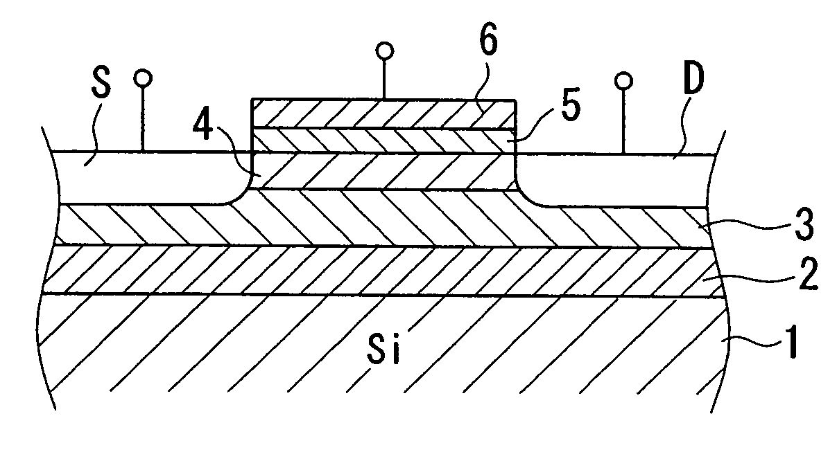
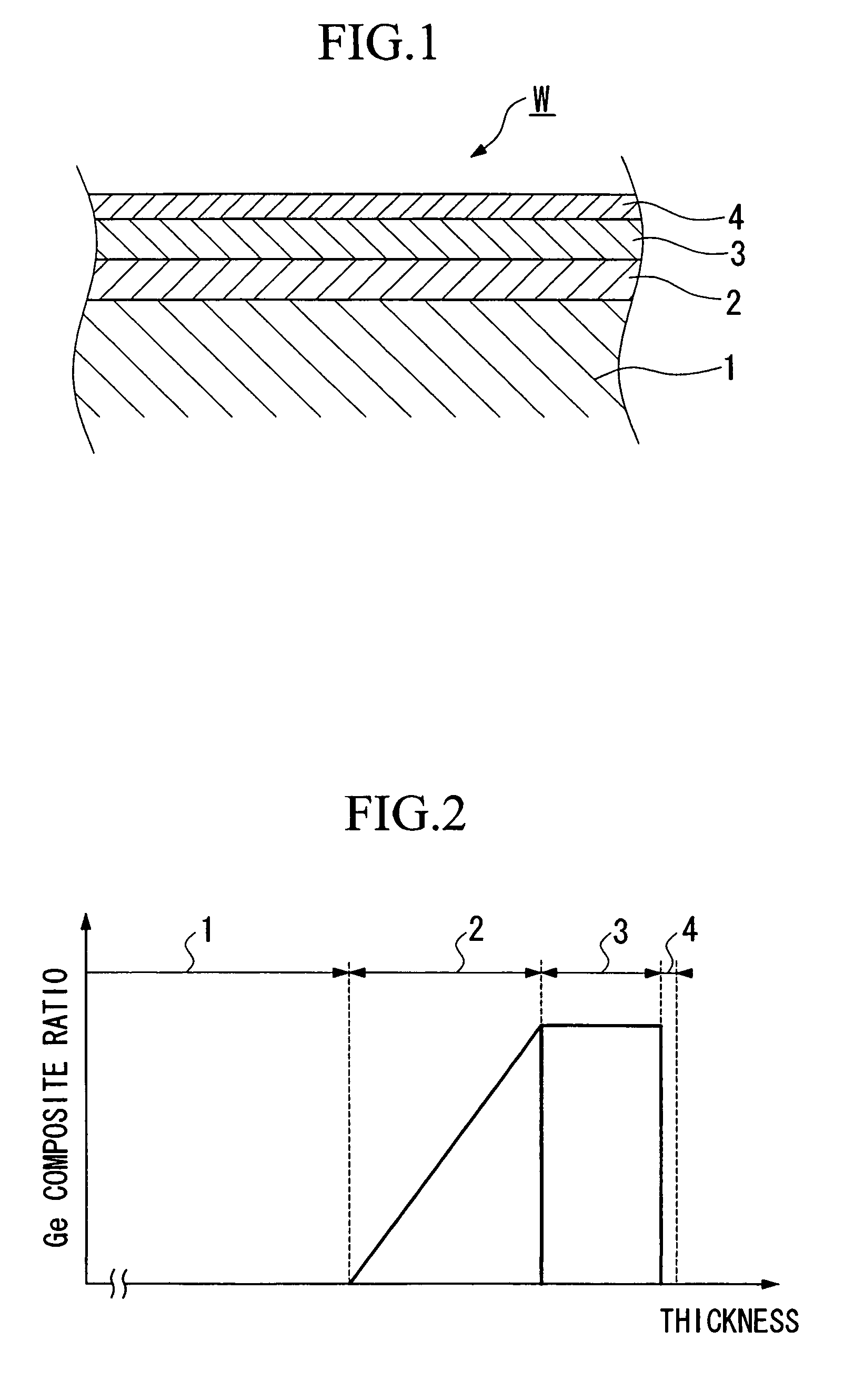
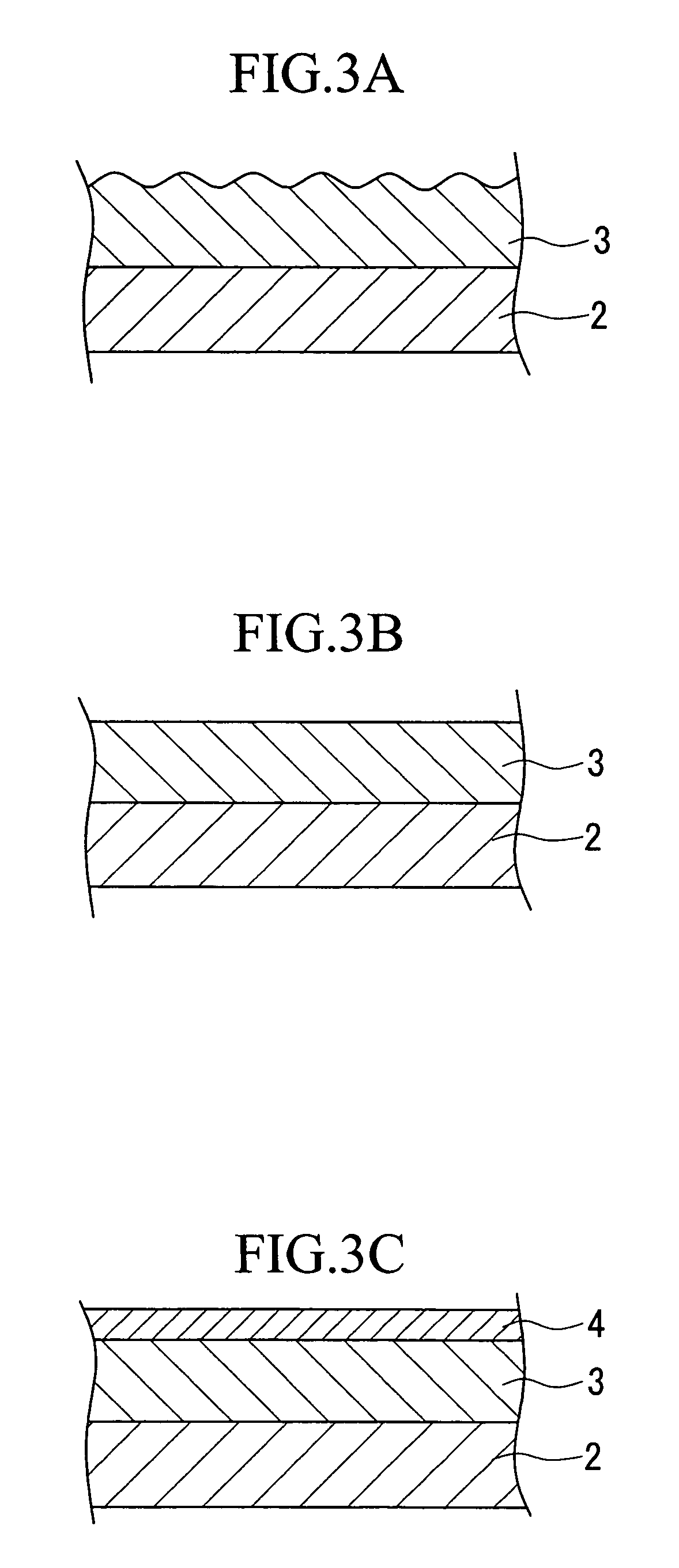
[0044]The following provides a detailed explanation of worsening of surface and interface roughness in the case of heat treatment based on the aforementioned embodiments with reference to FIGS. 5A and 5B and FIGS. 6A and 6B.

[0045]Graphs of surface roughness and the power spectrum of that roughness are shown in FIGS. 5A and 5B, respectively, for the case of performing heat treatment consisting of an annealing temperature of 1000° C. and annealing time of 10 minutes during deposition of the second SiGe layer 3 based on the aforementioned embodiments, and depositing the remaining second SiGe layer 3 after the heat treatment. Furthermore, surface roughness was measured using a Nomarski surface roughness measuring device. In addition, graphs of surface roughness and the power spectrum of that roughness in the case of not performing heat treatment are similarly shown in FIGS. 6A and 6B as a comparative example. In the aforementioned graphs of the power spectra of surface roughness, the wa...


PUM


Abstract

The present invention relates to a semiconductor substrate production method, field effect transistor production method, semiconductor substrate and field effect transistor which, together with having low penetrating dislocation density and low surface roughness, prevent worsening of surface and interface roughness during heat treatment of a device production process and so forth. A production method of a semiconductor substrate W, in which SiGe layers 2 and 3 are formed on an Si substrate 1, is comprised of a heat treatment step in which heat treatment is performed either during or after the formation of the SiGe layers by epitaxial growth, at a temperature that exceeds the temperature of the epitaxial growth, and a polishing step in which irregularities in the surface formed during the heat treatment are removed by polishing following formation of the SiGe layers.

Description

TECHNICAL FIELD[0001]The present invention relates to a production method of a semiconductor substrate used in high-speed MOSFET and other devices, a field effect transistor production method, a semiconductor substrate and a field effect transistor.BACKGROUND ART[0002]High-speed MOSFET, MODFET and HEMT have been proposed in recent years in which an epitaxially grown strained Si layer interposed with an SiGe (silicon-germanium) layer on an Si (silicon) substrate is used for the channel region. In this strained Si-FET, tensile strain occurs in the Si layer due to the SiGe having a larger lattice constant than the Si, and as a result, the band structure of the Si changes, degeneration is removed and carrier mobility increases. Thus, as a result of using this strained Si layer as a channel region, speed can be increased to about 1.3 to 8 times faster than ordinary speeds. In addition, since ordinary Si substrates manufactured by the CZ method can be used for the substrates, high-speed C...

Claims


Application Information

Patent Timeline
Patent Type & Authority Patents(United States)
IPC IPC(8): H01L21/336H01L21/205H01L21/20H01L21/337H01L29/10H01L29/165H01L29/78
CPCH01L21/02381H01L21/0245H01L21/02502H01L29/66916H01L21/0262H01L29/1054H01L29/165H01L21/02532H01L21/18
Inventor SHIONO, ICHIROMIZUSHIMA, KAZUKIYAMAGUCHI, KENJI
Owner SUMITOMO MITSUBISHI SILICON CORP
Why Eureka
Try Eureka